THIN-FILM COATINGS: OSA contest highlights optical coaters' abilities
Every three years, the Optical Society (OSA) holds the Optical Interference Coatings (OIC) conference, always at a location that somehow is also attractive for vacationing (Banff, AB, Canada, in 2001; Tucson, AZ, in 2004, 2007, and 2010; and Whistler, BC, Canada, in 2013). And every time the OIC is held, the results of a unique contest are announced.
In the humbly named Manufacturing Problem Contest, contestants must design and fabricate an optical coating that fits the design requirements—different every time, and always unusual and difficult—of the contest’s organizers. The results of the fifth Manufacturing Problem Contest, which were announced at the OIC last year in Whistler, have now been published in detail.1
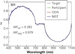
A spectral transmittance target of—what?
The design target for last year’s contest is far-removed from any ordinary (and practical) filter design, but that’s the point—to push boundaries and learn from the process. The spectral shape of the normal-incidence transmittance target is an upward-pointing semicircle connected by a horizontal line segment to a downward-pointing semicircle (see Fig. 1). The spectral region spans 400 to 1100 nm—a very broad span, and twice that of the optical filters in the OIC’s previous contests.
The 50 × 50 × 4 mm substrates were of N-BK7 optical glass donated by Edmund Optics (Barrington, NJ). The transmittance of the filter was defined at the total transmission, giving the contestants the latitude to create two separate thin-film stacks, one for each side, that together create the filter. A merit function (MF) was defined and used to rate both the calculated and the measured filter performance.
Contestants had free rein in choosing coating materials, design, and number of layers, as well as the manufacturing and monitoring methods. The contest organizers encouraged the contestants to try a wide variety of approaches, as the contest is intended to expand the knowledge of the thin-film-coating community. Judging of the entries was based entirely on the MF resulting from normal-incidence spectral measurements done by Optical Data Associates (ODA; Tucson, AZ) and the National Institute of Standards and Technology (NIST; Gaithersburg, MA).
Results
Seventeen samples were received from 15 separate teams from North America, Europe, and Asia. The samples were anonymized (assigned random sample numbers) and sent to ODA and NIST (neither ODA nor NIST were allowed to be contestants). Both ODA and NIST used UV-VIS-NIR spectrophotometers for their measurements; ODA’s was the Cary 5000, made by Agilent (Santa Clara, CA), while NIST’s was a Lambda 1050 by PerkinElmer (Waltham, MA).
All participants used two materials—one high-index and the other low-index—in their designs. Beyond this, though, the designs varied widely, ranging from 26 to 608 layers, from 1.859 to 23.099 μm in thickness, from 0.283 to 1.960 for calculated MFs, and from 0.979 to 18.015 for measured MFs (see Fig. 2). Three of the samples had coatings on both surfaces, while the other 14 had a coating on only one.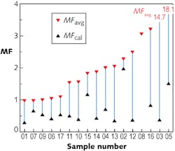
While the teams themselves were identified in the contest, the evaluation results were not linked to the contestants, except for the three best-performing samples. The makers of these samples were: Eric Nybank of JDSU (Santa Rosa, CA); Zach Gerig of Advanced Thin Films (Boulder, CO); and Masaki Kato of Nikon Corporation (Tokyo, Japan). The MFs for all three samples were almost identical.
A note from the organizers about the next contest: “We would like to remind future participants that information about the Manufacturing Problem Contest is normally available on the OSA website the year before the OIC conference—this will be October 2015 for the 2016 contest. The deadline for submitting samples is around March 1 [2016].”
REFERENCE
1. L. Li et al., Appl. Opt., 53, 4, A248 (February 1, 2014).
About the Author

John Wallace
Senior Technical Editor (1998-2022)
John Wallace was with Laser Focus World for nearly 25 years, retiring in late June 2022. He obtained a bachelor's degree in mechanical engineering and physics at Rutgers University and a master's in optical engineering at the University of Rochester. Before becoming an editor, John worked as an engineer at RCA, Exxon, Eastman Kodak, and GCA Corporation.