SOLID-STATE DEEP UV EMITTERS/DETECTORS: Zinc oxide moves further into the ultraviolet
DAVID J. ROGERS, PHILIPPE BOVE, ERIC V. SANDANA, FERECHTEH HOSSEINI TEHERANI, RYAN MCCLINTOCK, and MANIJEH RAZEGHI
Zinc oxide (ZnO) is a remarkable, multifunctional semiconducting material with a direct, wide bandgap energy (Eg ~ 3.4 eV), intrinsically high transparency over the whole visible range, and a resistivity that can be tuned from semi-insulating right through to semi-metallic by doping.1 It also presents one of the highest piezoelectric responses of any semiconductor and has a relatively high thermoelectric figure of merit. Moreover, it has been judged to be biocompatible and has been approved for human consumption (in products such as vitamin pills) by the U.S. Food and Drug Administration.
These distinctive properties have led to a number of industrial applications for ZnO. A recent Nanomarkets (Glen Allen, VA) study estimated that the ZnO-based optoelectronics market was already worth over half a billion dollars in 2010 and forecast to grow to more than 2.3 billion dollars by 2017, at which point over 65% of the market is to be made up of emerging applications: predominantly photovoltaics, displays, light-emitting diodes (LEDs), and sensors (gas, ultraviolet [UV] light, and biological).
In photovoltaics, ZnO is currently displacing indium tin oxide for use as a transparent conducting electrical contact due to recent improvements in conductivity obtainable with aluminium-doped ZnO, combined with processing, cost, and toxicity advantages.2
For display applications, the greatly superior electron mobilities and current on/off ratios that can be obtained with ZnO-based transparent thin film transistors have opened up the potential for replacing amorphous silicon select field-effect transistors in both active-matrix organic LED and liquid-crystal-based displays/screens.
ZnO benefits
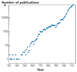
The emerging potential of ZnO for UV emitter and detector applications is the result of a long, concerted, and fruitful R & D effort that culminated in more than 7000 publications in 2012 (see Fig. 1). In the early years, the research focused principally on the crystal structure and the basic physical/optical properties. The upturn in output from the early 1990s was most probably triggered by the burgeoning technical and commercial success of gallium nitride (GaN) in optoelectronic devices.
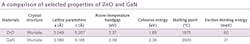
A link was made between ZnO and GaN because they are very similar materials with the same wurtzite crystal structure, comparable lattice-constants/bandgaps, and high cohesive-energies/melting points (see table). There are some important differences, however. In particular, ZnO is considered to be a potentially superior material for use in LEDs and laser diodes because of its much larger exciton binding energy (60 meV) compared to 21 meV for GaN (thermal energy at room temperature is about 25 meV). This means that we can expect brighter and more robust excitonic-based ZnO emitters.
Furthermore, wet etching is possible for ZnO with nearly all dilute acids and alkalis (greatly simplifying device processing), whereas GaN requires hydrofluoric (HF) acid or plasma etching. Zinc oxide is also relatively abundant (unlike Ga), so ZnO cost is low. Finally, high-quality ZnO films can be grown more readily on mismatched substrates (due to the particularly compliant nature of ZnO), and bulk ZnO substrates have better availability than their GaN equivalents.
Another upturn in ZnO-related publications after the year 2000 can be associated with several key findings, including the demonstration of stimulated excitonic emission at temperatures higher than 550 K, reports of p-type doping, and the emergence of ZnO as an important nanomaterial (see Fig. 2). A Thomson-Reuters market survey, published in 2010, recorded more publications dedicated to nanostructured ZnO than to carbon nanotubes. This is primarily due to the multifunctional nature of ZnO, the ease of fabricating nanostructures by various techniques (including wide-area, low cost chemical growth), and the extremely large family of nanostructure types that can be obtained.
LEDs and lasers
In spite of the potential of ZnO-based LEDs, their commercialization has been hampered by issues of simultaneously reducing intrinsic n-type doping and incorporating/activating sufficient acceptors. The native donor compensation is usually associated with defects inherent to oxygen-deficient ZnO (O vacancies and Zn interstitials) plus unintentional impurity incorporation (hydrogen, in particular).
Since 1999, however, there have been a multitude of reports of p-type doping.3 These efforts have used a wide range of growth techniques, substrates, and acceptor doping approaches with a variety of group-I, -IV, and -V elements, co-doping, and impurity/defect complexes, respectively. The most commonly reported acceptor dopants are nitrogen (N), arsenic (As), phosphorus (P), and antimony (Sb). And native acceptor defect doping (with Zn vacancies and O interstitials) has been targeted through oxidant-rich growth.
There have been many demonstrations of blue and near-UV ZnO homojunction LEDs as well, and state-of-the-art performance (70 μW at 30 mA) can be compared to that of GaN-based LEDs in the mid-1990s.4 Issues to be addressed include an asymmetry in the n- and p-type carrier concentrations, relatively low p-type mobilities, and poor electrical contacts.
There have also been many reports of low-threshold, high-gain UV lasing from ZnO-based materials and devices under optical pumping, including room-temperature UV photonic crystal lasing and random lasing from self-forming laser cavities.5 What's more, patterned ZnO-based microcavities have shown promise for use as low-threshold surface-emitting polariton lasers. And recently, there have been reports of electrically pumped ZnO lasers, although relatively low doping levels limit the performance.
Deep-UV emitters and detectors
Alloys of GaN with aluminum (AlxGa1-xN) have been widely explored for emission and detection of UV light (see Fig. 3).6 This material system is plagued by several problems, however, including large dislocation densities, low n-type and p-type doping efficiency, low conductivity, and lattice/thermal expansion mismatches that lead to cracking. As a result, efficiency falls off dramatically with increasing Al content, and there has been limited success in demonstrating solar-blind UV photodetectors (SBPDs; i.e., in the 240–290 nm range) with low background signals and high quantum efficiencies.
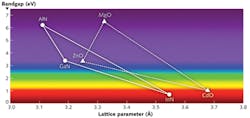
Alloys of ZnO with magnesium (MgxZn1-xO) have been explored as an alternative to (Al)GaN and are now commercially available.7 The Mg ion has a similar radius to that of Zn, so there are less strain and efficiency drop-off concerns than for (Al)GaN.
The commercialization of (Mg)ZnO-based UV devices will most probably begin with detector applications rather than emitters because photodetector technologies that do not require p-type doping (such as photoconductors, Schottky diodes, metal-semiconductor-metal devices, and surface acoustic wave devices) have already been demonstrated.
UV photodetectors are envisioned for detection of weak UV signals in applications such as flame/chemical/biological-agent detection, UV astronomy, next-generation missile warning/guidance systems, hostile fire identification, environmental monitoring, and non-line-of-sight communications. To minimize false alarms and background clutter, many of these systems operate in the solar-blind SB portion of the UV spectrum.
While (Al)GaN-based detectors work well in the near-UV, current commercial SB detection systems are usually based on photomultiplier tubes (PMTs) with cesium telluride (Cs2Te) photocathodes. These have a detection tail out to 325 nm, which overlaps with the solar UV spectrum, making these sensors not truly blind to solar background radiation, however. Thus filters and complex optics are usually required to achieve true SB status. State-of-the-art PMT detectors have a peak detective quantum efficiency of 15%. In addition, the high-voltage vacuum tubes are bulky, fragile (mechanically and electrically—high flux can physically damage the internal electron multiplication grids), expensive, and require high operating voltages.
Solid-state SBPDs promise performance, size, and cost advantages compared to PMTs. Such arrays have no moving parts, are intrinsically radiation hard, and potentially offer higher quantum efficiency, higher selective sensitivity, extended lifetimes, lower noise, and lower-power requirements. Direct-gap semiconductors also offer very sharp cutoffs (<10 nm per decade) compared to existing photocathodes (around 25 nm per decade). This allows them to be made significantly more solar blind while maximizing the capture of the SB portion of the UV emission.
For fabricating (Mg)ZnO-based SBPDs, Mg content should be at least 45 at %, but many studies have found that phase segregation of rock-salt phase MgO appears when Mg content is over 36 at %. Recently, however, single-phase wurtzite layers with Mg concentrations over 49 at % were prepared through strain engineering at the substrate interface by means of buffer layers (ZnO and strontium titanate—SrTiO3—or bulk ZnO substrates).8-10
Furthermore, it has been reported that Mg alloying facilitates the task of p-type doping. Two main reasons are put forward for this. First, the addition of Mg in ZnO shifts the conduction band edge to a higher energy, which increases the activation energy of the donor states and thereby reduces the n-type background electron concentration.11 Second, the Zn vacancy (acceptor) concentration has been observed to increase with Mg concentration, which boosts the increment of hole concentration and p-type conduction.12 Another intrinsic advantage compared to (Al)GaN is the even greater resistance of (Mg)ZnO to ionizing radiation and high-energy particles.
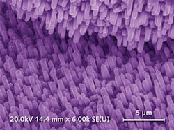
Current (Mg)ZnO-based SBPD research has recently extended to nanostructures. These offer higher crystal quality, non-polar core-shell junctions, better compatibility with silicon, very wide-area low-temperature chemical growth on mismatched substrates, an advantageous size-related blue shift, reduced device processing (inter-digit patterning can be circumvented), plus intrinsic antireflection advantages. Indeed, ZnO nanowire-based UV PDs have been widely reported in the literature, and such devices have already shown larger gain bandwidth compared to bulk devices, very high photoconductive gains (up to approximately 108), single-photon sensitivity, and Schottky barrier contacts, which eliminate long transients and thereby boost response speed.
In summary, (Al)GaN-based deep-UV solid-state emitters and detectors have shown cracking and disappointing efficiencies, so (Mg)ZnO-based alternatives are being investigated as possible substitutes.
This effort has been boosted by recent advances in strain engineering at the substrate interface, which have allowed stabilization of single-phase wurtzite (Mg)ZnO with up to 49% Mg.
Moreover, the p-type doping issues of unalloyed ZnO (associated with native donor defect compensation and insufficient acceptor concentrations) are significantly reduced in (Mg)ZnO because of the higher activation energy of the donor state and the increase in zinc vacancy acceptor density with Mg content. For detector applications, p-type doping is not a requisite, however, and nanostructured (Mg)ZnO-based devices have already demonstrated the promise of improved performance, simplified processing, wider areas, and lower cost compared to their thin-film (Al)GaN-based equivalents.
ACKNOWLEDGEMENTS
The authors wish to thank Carlos Lee (director general of the European Photonics Industry Consortium; Paris, France) for his support in this work, professor Seong-Ju Park of the Gwangju Institute of Science & Technology (GIST; Gwangju, Korea) for useful exchanges on the state-of-the-art in p-type ZnO doping and Professor Jose-Luis Pau of Universidad Autónoma de Madrid (Madrid, Spain) for discussions on the state-of-the-art in nanostructured UV photodetectors.
REFERENCES
1. D. J. Rogers et al., Proc. SPIE, 7605, 76050K-1 (2010).
2. D. J. Rogers and F. Hosseini Teherani, Encyclopedia of MaterialsScience& Technology, 1–5, Elsevier, Oxford, England (2010).
3. J.-C. Fan et al., Prog. Mater. Sci., 58, 874 (2013).
4. K. Nakahara et al., Appl. Phys. Lett., 97, 013501 (2010).
5. A.-S. Gadallah et al., Appl. Phys. Lett., 102, 171105 (2013).
6. M. Henini and M. Razeghi, III-Nitride Optoelectronic Devices, Chapter 1, Elsevier, England (2004).
7. D. J. Rogers et al., Proc. SPIE, 8626, 862601 (2013).
8. S. Fujita et al., Phys. Status Sol. B, 241, 599 (2004).
9. W. Yang et al., Appl. Phys. Lett., 82, 3424 (2003).
10. Q. Zheng et al., Appl. Phys. Lett., 98, 221112 (2011).
11. P. Wang et al., Appl. Phys. Lett., 89, 202102 (2006).
12. Y. F. Lee et al., Appl. Phys. Lett., 91, 232115 (2007).
David J. Rogers is CTO, Philippe Bove is COO, Eric V. Sandana is an engineer, and Ferechteh Hosseini Teherani is CEO at Nanovation, 8 route de Chevreuse, Chateaufort, 78117 France; email: [email protected]; www.nanovation.com. Ryan McClintock is an associate professor and Manijeh Razeghi is Walter P. Murphy professor of Electrical and Computer Engineering and director at the Center for Quantum Devices at Northwestern University, 633 Clark St., Evanston, IL 60208; www.northwestern.edu.