UV DETECTORS: Zinc-oxide materials and their alloys redefine UV sensing
SHIVA HULLAVARAD and NILIMA HULLAVARAD
Zinc oxide (ZnO) is a wide-bandgap optoelectronic material belonging to the II-VI family of semiconductors with a direct-energy bandgap of 3.3 eV at room temperature. It crystallizes in a wurtzitic hexagonal crystal structure in which zinc and oxygen planes are alternately stacked along the c-axis direction. The 1957 review article “Zinc Oxide Rediscovered” by H.E. Brown lists more than 40 applications of ZnO as diverse as brake liners for automobiles, coatings for industrial markets, and for consumer health and beauty products.1 Since then, ZnO has been the subject of intense scientific interest for almost half a century with early emphasis on its fluorescent and photoconductive properties.2, 3
Compared to its gallium nitride (GaN) counterpart, ZnO offers easier material preparation, tunability of its optoelectronic properties, and inexpensive and scalable device fabrication methods (see Table 1). Researchers’ curiosity in exploring wide-bandgap materials to achieve blue and ultraviolet (UV) light emission and detection from solid-state junctions paved the way for discovery of blue light-emitting diodes (LEDs) and has resulted in new techniques for creating novel device structures and optimizing device properties through different semiconductor growth scenarios.
| Parameter/characteristics | MgxZn1-xO | AlxGa1-xN |
| Bandgap | 3.3 to 5.0 eV | 3.3 to 6.2 eV |
| Exciton binding energy | 60 meV (ZnO) | 25 meV (GaN) |
| Temperature for growth of oriented thin films for devices | Room temperature (25°C)-500°C | 850 to 1100°C |
| Fabrication/growth methods | Low-cost sputtering, laser ablation, CVD, evaporation (also by MBE and MOCVD but may be expensive) | Expensive methods such as MBE and MOCVD |
| Substrates for heteroepitaxy | Sapphire, MgO, SrTiO3 | Sapphire, SiC |
| Fabrication on low-cost substrates: glass polymers (poly films) | Highly possible | Very difficult |
| Etching | Easy to etch with wet process | Only with reactive dry etching |
| Doping | n-type well established, p-type demonstrated, but results sporadic | n- and p-type well established |
UV sensing
When a ZnO surface is exposed to oxygen or air, oxygen is adsorbed on its surface. Each adsorbed oxygen ties up an electron from the conduction band, reducing the number of electrons available for conduction near the surface. The exposure to oxygen thus reduces ZnO conductivity and the device exhibits higher resistivity. An electron-hole pair is generated when a photon of energy equal to or higher than the bandgap is absorbed in the material. Adsorbed oxygen and the photo-generated hole contribute to local charge neutrality and free up the photo-generated electron to enhance the conductivity of the device.
Like other semiconductor-based UV sensors, ZnO sensors are fabricated by depositing a thin film of ZnO by any physical or chemical-vapor deposition techniques on select substrates. Typically, ZnO and magnesium ZnO (MgZnO) UV sensors are fabricated using a metal-semiconductor-metal (MSM) configuration. The next step is to fabricate inter-digitated (IDT) contacts on the ZnO thin film using standard photolithographic techniques in such a way that the IDT spacing is less than the carrier recombination length, ensuring that photo-generated carriers are collected before they recombine to produce a measurable signal output. Our group has fabricated IDT metal electrodes on ZnO using 150 nm thick chromium/gold (Cr/Au) bilayers by conventional photolithography that are typically 250 µm long and 5 µm wide with an inter-electrode spacing of 5 µm.
For measuring UV light-sensing properties, a xenon (Xe) light source with a broad output in the 200–500 nm region, a monochromator, and a current amplifier are used. To date, there has been a tremendous research effort in fabricating ZnO sensors for UV detection in various configurations; gas- and biological-sensing applications are also being explored.
Bandgap tunability with magnesium alloys
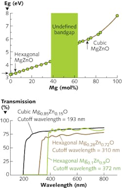
Zinc oxide offers additional advantages over GaN in its ability to provide wider bandgaps up to 7.5 eV by alloying with magnesium oxide (MgO); 6 eV is the typical bandgap for the highest aluminum (Al) fractions in AlGaN. In addition, MgZnO exhibits the same fundamental material advantages as those of pure ZnO. By varying the Mg composition, the bandgap can be tuned from 3.3 to 7.8 eV for wurtzite and cubic structured MgxZn1-xO, extending the cutoff wavelengths from UV-A (320–400 nm) to UV-B (280–320 nm) and UV-C (200–280 nm) regions (see Fig. 1). This wide sensing range is expected to enable MgxZn1-xO UV detectors to be used in many applications such as solar UV radiation monitoring, ultrahigh-temperature flame detection, and airborne missile warning systems.4
For MgO composition of <36% in ZnO, MgZnO crystallizes into a hexagonal wurtzite crystal structure. The maximum achievable bandgap with the hexagonal MgZnO is 4.25 eV. Further increase of MgO in ZnO leads to mixed-phase regions for MgO concentrations from 37–61% and the bandgaps of the resulting thin films in this region are < with multiple absorption edges occurring in the UV-absorption spectra.5 This mixed-phase region has drawn specific interest for developing rock-salt MgZnO thin films that are believed to provide a metastable structure favorable for p-type dopant activation. An increase in MgO concentrations above 62% leads to a cubic MgZnO structure with bandgaps ramping up from 5.5 to 7.5 eV.
The characteristic feature of ZnO- and MgZnO-based materials is that of sharp UV absorption and constant blue shift in absorption edge as a function of Mg composition in ZnO. The transmission spectra of MgxZn1-xO thin films for x = 0.15, 0.28, and 0.90 corresponds to hexagonal (x = 0.15, 0.28) and cubic (x = 0.90) structures with 80% transmission and sharp absorption. The sharpness of the transmission spectra also reveals the clear band edges in the material, with strong absorption at cutoff wavelengths of 372, 310, and 193 nm corresponding to bandgaps of 3.3, 4, and 6.4 eV, respectively. The sensitivity and tunability of ZnO and MgZnO alloys with optical absorption in the UV and deep-UV regions has pushed ZnO and its alloys to the forefront of UV detection.
Epitaxy and nanostructured devices
It is imperative that ZnO and MgZnO films are grown on lattice-matched substrates to reduce the interface dislocation density because the quantum efficiency of many optoelectronic devices depends on the defect densities.6 It is therefore important to study the effect of substrate (lattice structures, orientation, lattice constants, and surface chemistry) on the growth dynamics of thin films.
Most ZnO and MgZnO alloy thin films have been deposited on basal plane (0001) sapphire substrates, which have 17% lattice mismatch with respect to ZnO (see Table 2). Devices fabricated on lattice-matched substrates (hexagonal film on hexagonal substrate, cubic film on cubic substrate) provide better UV-to-visible rejection ratio, a parameter that defines UV sensitivity.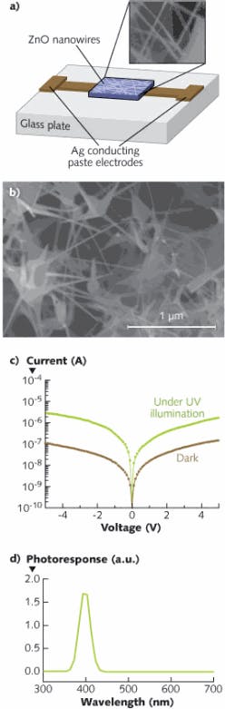
Nanowires offer one very important advantage for light detection by virtue of narrow dimensions and proximity to each other in an assembly, eliminating the cumbersome process of defining IDTs by expensive photolithography techniques that involve at least six to eight cleanroom processes.9 We can essentially form ZnO UV light sensors by using a simple process that only requires a glass plate and conducting silver paint to form electrodes separated by a gap of 0.1 mm (see Fig. 2). The ZnO nanostructures dissolved in a toluene solution are placed drop-wise between the gap and allowed to dry. Sensors fabricated from ZnO nanostructures consisting of microspheres in a network of nanowires are more sensitive to the incoming light. Such multishape ZnO nanostructured UV sensors exhibit 100 mA/W photoresponsivity. It should also be noted that the fusion of different nanostructure shapes and dimensions could lead to broader spectral performance and a completely different domain of applications.10
Although initial results for nanostructured ZnO sensors are promising, improvements are needed in materials technology with an emphasis on doping and fabrication of stable homo- and hetero-p-n junctions and metal-semiconductor ohmic and Schottky contacts to develop reliable devices that will serve existing and emerging applications.
ACKNOWLEDGMENT
Authors acknowledge the financial support from the U.S. Defense Advanced Research Projects Agency (DARPA) at University of Alaska Fairbanks under contract number N66001-08-C-2081.
DISCLAIMER
The views, opinions, and/or findings contained in this article/presentation are those of the author/presenter and should not be interpreted as representing the official views or policies, either expressed or implied, of the Defense Advanced Research Projects Agency or the Department of Defense. Distribution Statement “A” (Approved for Public Release, Distribution Unlimited)
REFERENCES
1. H.E. Brown, “ZnO Rediscovered,” The New Jersey Zinc Co., New York, NY (1957).
2. F.A. Kroger and H.J. Vink, J. Chem. Phys. 22, 250 (1954); doi:10.1063/1.1740044.
3. S.E. Harrison, Phys. Rev. 93, 52 (1954).
4. S.S. Hullavarad et al., J. Vac. Sci. Technol. A 23, 982 (2005).
5. W. Yang et al., Appl. Phys. Lett. 82, 3424 (2003).
6. A. Ohtomo and A. Tsukazaki, Semicond. Sci. Technol. 20, S1 (2005).
7. J. Johnson et al., Nature Materials 1, 106 (2002).
8. S. Kan et al., Nature Materials 2, 155 (2003).
9. S.S. Hullavarad et al., Nano Scale Research Letters; doi 10.1007/s11671-007-9048-6 (2007).
10. S.S. Hullavarad and N.V. Hullavarad, Proc. 8th IEEE Conf. on Nanotechnology (NANO 08), Arlington, TX, 44-47, doi: 10.1109/NANO.2008.21 (2008).
Shiva Hullavarad and Nilima Hullavarad are research assistant professors at the Office of Electronic Miniaturization, University of Alaska Fairbanks, 3330 Industrial Ave., Fairbanks, AK 99701; e-mail: [email protected]; www.uaf.edu.