III-V space-based PV cells could go terrestrial
Photovoltaic (PV) cells made from III-V semiconductor materials have the highest demonstrated optical-to-electrical conversion efficiency (around 40%); however, the epitaxial-growth process used to fabricate these cells is expensive and slow, formerly limiting them to space-based and concentrating PV applications. But a new vapor-liquid-solid (VLS) growth process from University of California, Berkeley scientists makes it possible to grow polycrystalline indium phosphide (InP) thin films on molybdenum (Mo) substrates, clearing a path towards the fabrication of large-area, ultra-efficient PV cells for terrestrial applications.
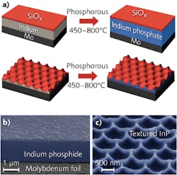
The growth process begins with deposition of indium films (with tunable thickness from 0.2 to 2 μm) on 25-μm-thick Mo foils via either electron-beam evaporation or electroplating, followed by e-beam evaporation of a 50-nm-thick silicon oxide (SiOx) cap. This stack is then heated in hydrogen to a temperature that melts the indium, allowing introduction of a phosphorous vapor that diffuses into the indium and, upon cooling, results in the precipitation of solid InP crystals. Besides planar films, textured films with improved carrier collection can be fabricated by introducing 1-μm-diameter silica beads, for example. After etching away the SiOx cap, luminescence and photogenerated current levels were found to be comparable to or better than copper indium gallium selenide (CIGS) thin-film PV materials. Contact Ali Javey at [email protected].
About the Author

Gail Overton
Senior Editor (2004-2020)
Gail has more than 30 years of engineering, marketing, product management, and editorial experience in the photonics and optical communications industry. Before joining the staff at Laser Focus World in 2004, she held many product management and product marketing roles in the fiber-optics industry, most notably at Hughes (El Segundo, CA), GTE Labs (Waltham, MA), Corning (Corning, NY), Photon Kinetics (Beaverton, OR), and Newport Corporation (Irvine, CA). During her marketing career, Gail published articles in WDM Solutions and Sensors magazine and traveled internationally to conduct product and sales training. Gail received her BS degree in physics, with an emphasis in optics, from San Diego State University in San Diego, CA in May 1986.