FOCAL PLANE ARRAYS: SWIR InGaAs FPA enables photon emission failure analysis
RAF VANDERSMISSEN and PATRICK MERKEN
Specially designed focal plane arrays (FPAs) are required to obtain the lowest possible noise and highest sensitivity in applications such as high-resolution spectroscopy, nanotube fluorescence imaging, and especially for photon emission measurements such as in semiconductor failure analysis (see photo above). Such a design may also be critical in other very low-light-level, short-wavelength infrared (SWIR) and visible-to-near-infrared (VisNIR) imaging tasks.
To meet requirements for low dark current, low noise, and sensitivity in the SWIR range, Xenics developed an indium gallium arsenide (InGaAs) detector, the XFPA-1.7-640-LN2, optimized for 77 K operation. The circuitry is based on a source-follower detector (SFD) read-out, which provides high sensitivity at a resolution of 640 × 512 pixels and a pixel pitch of 20 μm.
The frame rate is 2.5 Hz (in 4-output mode), which can be increased when a smaller region of interest is selected. Nondestructive read-out mode simplifies operation when long integration times are used. Liquid nitrogen (LN2) cooling allows for very low noise (<20e-). A low dark current (<5e-/s/pixel) can also be achieved at these low temperatures. The sensitive wavelength band of the device covers the region from 0.9 to 1.6 µm (optional 0.4 to 1.6 µm).Sensor design
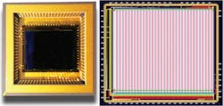
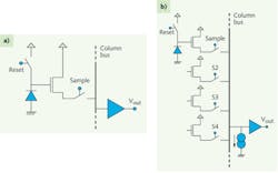
The light detectors are integrated along with the silicon-based ROIC, which utilizes Xenics’ in-house hybridization technology (see Fig. 1). Pixel topology is based on an SFD stage, which is known for its excellent noise performance. The basic (simplified) pixel schematic is shown in Fig. 2a.The SFD’s main advantage is design simplicity and the ability to integrate charge without the need to be powered. Therefore the SFD is a good choice for large-format arrays with small pixel dimensions. Another advantage is the fact that very few elements are present in the pixel that will reduce the so-called Narcissus effect, which can substantially degrade detector performance in low-temperature applications.
The main disadvantage of the SFD is the change in the input node voltage that occurs as charge is collected on the input node capacitance of the circuit. However, this is not a serious drawback because the intended use is low-temperature operation, where the impact of unstable bias is greatly reduced, if not completely absent.
All pixels are interconnected via a common column bus and sequentially read out through an analog multiplexer circuit. Interconnect and signal paths are laid out in a low-complexity fashion to optimize noise performance (see Fig. 2b).
Operational modes
The sensor device offers two distinct modes of operation: NDR (nondestructive readout, also known as integrate while read) and ITR (integrate then read). Timing diagrams for both modes of operation are shown in Fig. 3.NDR mode operation starts with a simultaneous global reset of the entire array. All pixels begin simultaneously with the integration of IR induced carriers. However, the pixels are not read out simultaneously in this mode (the integration time of first and last pixel is different). Therefore, the external electronic circuitry always uses the first frame read-out as reference for the subsequent frames. As leakage is very low and integration times are long, several frames can be used to build up the resulting image using advanced multisample signal-acquisition techniques.
In ITR mode all pixels start integration at the same time and then are sequentially read out. Integration time here is simply the time between Reset and Sample moments.
The sensor device has four different (selectable) outputs, which can drive capacitive loads. The sensor allows operation in a window-of-interest (WOI) or Windowing mode. To ease cooling measures and device operation, a temperature sensor was integrated. The chip consists of the actual FPA and the ROIC detector interface combined with a digital circuit for multiplexing and signal transfer, as well as an analog interface and test topologies.
Nanotube imaging
Nanotube fluorescence is typically investigated in nanotechnology imaging research. The ultimate goal is to create faster nanoelectronic devices as well as ultrastrong and extremely lightweight materials with advantageous structural features. Of particular interest are nanotubes, which are formed when carbon atoms bond to one another to establish planar hexagonal rings.
The formation of nanotubes is widely investigated with the aim of improving production processes. When produced on a perfect molecular level, fullerene tubes offer revolutionary electrical, thermal, and mechanical properties at the nanometer scale. Researchers are also interested in the optical properties of nanotubes as they have potential applications as fluorescent tags in chemical and biological systems.
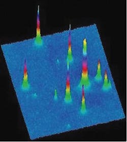
The availability of LN2-cooled InGaAs cameras with high sensitivity can now enable researchers to capture low-light fluorescence events in the SWIR region (900 to 1600 nm) stemming from nanomaterials (see Fig. 4).Quantum dot research
Quantum dot research is a relatively new field that targets new applications in optoelectronics and quantum information processing. Sensitive SWIR cameras are used here to investigate and better understand the physical properties of quantum dots.
The quantum dots can be regarded as “artificial atoms.” The photoluminescence of quantum dots is tunable by changing the dot size over a wide range, from the far infrared to deep ultraviolet.
Photon emission microscopy
Photon emission microscopy (PEM) can be used as a failure-analysis technique for the localization of defects in semiconductor devices. System sensitivity (in other words, InGaAs detector sensitivity) is key in such photon emission applications.
If the very faint emissions—in the 900-to-1600-nm wavelength band—that are typically caused by failure effects can be detected, then this technique can be used to quickly locate leaky junctions and other current leakage phenomena that generate light emissions.
Very sensitive InGaAs detectors, when equipped with LN2 cooling, have an extremely low dark current and low noise. They enable operation modes with long integration times and excellent signal-to-noise ratios.
Semiconductor failure analysis
In semiconductor failure analysis, photon emission microscopy has the potential for high-volume applications. High-end photon emission microscopes based on LN2-cooled InGaAs cameras can be used for fault localization in component fabs and foundries for production quality control, return merchandise authorization (RMA) control, and electronic design debug purposes.
Fault localization is the manufacturing step that attempts to isolate the defective areas on the die of failed units. It is a critical step since it dramatically reduces the area required for the analysis. Moreover, after characterizing a localized defect, the underlying failure mechanism can be further investigated.
Two main categories of fault localization exist: passive and active. Active techniques typically use a scanning ionizing beam (e.g., a laser beam) to stimulate the failure source. The most common passive technique is photon emission microscopy by means of sensitive (appropriately cooled) cameras. It relies on the fact that various types of failures will emit small amounts of light (photon emission, or also electroluminescence) when the failure is occurring.
Frontside chip or wafer analysis through a photon emission microscope faces limitations due to the growing use of multilevel metallization. This prevents photon emissions of the defects from reaching the detector. Backside chip or wafer analysis can benefit from the fact that silicon, the most common material in microelectronics, is fairly transparent for near-infrared light at wavelengths longer than 1100 nm (see photo at top of this page).
This is exactly the area where SWIR InGaAs cameras show an advantage based on their high quantum efficiency (QE) between 1000 and 1600 nm. Moreover, the lower operating voltages that characterize the ongoing miniaturization of microelectronic devices are causing a shift toward longer photon emission wavelengths, typically peaking between 1300 and 1500 nm.
FPAs vs. CCD for PEM
Silicon-based CCD detectors have been used extensively for photon emission microscopy. Especially scientific-grade, back-illuminated, cooled CCD detectors are used for backside chip and wafer analysis. However, CCD cameras at a wavelength between 300 and 1100 nm are effective only for observing photon emissions with energy transitions above the silicon bandgap. They do not allow the observation of intraband emissions above 1100 nm, where this emission is most intense.
Also, sub-bandgap emissions involving chemical impurities, physical defects, deep traps, and other recombination centers cannot be observed with CCD detectors. Furthermore, backside analysis requires a transmission through the silicon substrate, which is opaque to wavelengths below 1100 nm.
Consequently, InGaAs-based cameras are the best candidates for high-sensitivity photon emission applications in the 900-to-1600-nm band because of their QE. Especially with LN2 cooling, they exhibit very low dark current and noise levels, making them the most sensitive detectors in this band.
Spectral analysis of photon emission in the SWIR is a very promising field if one takes into account that each semiconductor failure mechanism may have its own spectral signature. This, however, requires the use of very sensitive detectors in the SWIR band in combination with high-end diffraction optics or, alternatively, a wavelength-tunable filter.
Raf Vandersmissen is CEO of sInfraRed–a Xenics company, Singapore, and Patrick Merken is with RMA Brussels and Xenics, Ambachtenlaan 44, BE-3001, Leuven, Belgum; [email protected]; www.xenics.com.


