LOW-LIGHT IMAGING: Novel back-illuminated CCD enhances low-light-level detection
Since their invention in 1969, CCDs have been used to detect faint light from entities that range from stellar objects at the edge of the known universe to nanospheres under a microscope—and practically everything in between. Key features that have enabled low-light CCD cameras to facilitate numerous breakthroughs in both the life sciences and physical sciences include greater than 90% peak quantum efficiency (QE), very low read noise of 2 e- rms or less, excellent linearity, 100% fill factor, and outstanding charge-transfer efficiency.
About ten years ago, a variant of CCDs known as electron-multiplying CCDs (EMCCDs) was developed. In addition to the features noted previously, EMCCDs are able to achieve subelectron read noise at high frame rates, allowing single-photon detection. Thus, CCD and EMCCD cameras are commonly the instruments of choice for scientific applications ranging from steady-state astronomical imaging to dynamic single-molecule imaging, and from widefield imaging to spectroscopy.
Types of CCDs and EMCCDs
Scientific-grade CCDs afford researchers a number of distinct technologies from which to choose. Primary CCD types include front-illuminated CCDs, standard (thinned) back-illuminated CCDs, and back-illuminated deep-depletion CCDs.
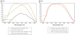
In a traditional front-illuminated CCD, light passes through the polysilicon gates that define a charge well at each pixel. As a result, front-illuminated devices typically offer only about 50% QE (or, in other words, the fraction of incident photons contributing to the signal). To improve QE, devices can be uniformly thinned via proprietary etching techniques to attain a thickness of approximately 10 to 15 µm and an image can be focused directly onto the photosensitive area of the CCD (the depletion region), where there is no gate structure. Compared to front-illuminated CCDs, these thinned back-illuminated devices have a higher QE across the entire visible spectrum with peak QE greater than 90%. To further improve QE, especially for near-infrared (NIR) imaging and x-ray applications, a bias voltage can be applied to a layer of high-resistivity silicon ranging from 50 to 300 µm in thickness in order to produce a "deeper" depletion region. This architecture allows longer-wavelength photons to interact within the layer, as opposed to merely penetrating it, ultimately helping to increase QE (see Fig. 1).
Electron-multiplying CCDs, meanwhile, are a relatively recent innovation. On-chip amplification of photoelectrons is used to boost signals above the read noise of the sensor (see Fig. 2). As a result, EMCCD cameras can achieve subelectron read noise even at video rates or higher. Not surprisingly, these cameras have become very popular for a variety of ultralow-light, high-frame-rate applications, including adaptive optics and single-molecule fluorescence imaging.![FIGURE 2. Electron-multiplying CCDs amplify electrons in an extended serial register through a process called impact ionization before they reach the output amplifier and subsequent electronics (left). The main benefit of the technology is a far better signal-to-noise ratio for signals below the read noise. A single-molecule fluorescence image is acquired with an EMCCD camera (right) [1].](https://img.laserfocusworld.com/files/base/ebm/lfw/image/2021/07/1004LFW7_2.60ed927ba9b38.png?auto=format,compress&fit=max&q=45?w=250&width=250)
Due to material processing and manufacturing complexities, EMCCDs are unable to realize deep-depletion technology commercially at this time. Unfortunately, for applications requiring NIR sensitivity and low "etaloning," this imposes significant limitations. (Etaloning is an unwanted phenomenon that causes interference patterns in back-illuminated sensors.) Front-illuminated EMCCDs, for instance, offer etalon-free imaging, but exhibit only 1/2 to 1/3 of the sensitivity of their back-illuminated counterparts. Conversely, back-illuminated EMCCDs suffer from etaloning in the NIR, though they have higher QE in this region.
New back-illuminated sensor technology
Researchers whose applications require low-light broadband photon detection have until recently had to choose between cameras that use either standard thinned back-illuminated or back-illuminated deep-depletion technologies. Although both of these options are capable of delivering extremely high sensitivity, their performance is nonetheless compromised to a certain extent by the limitations described in the preceding section.
Recently Princeton Instruments, Photometrics (Tucson, AZ), and e2v (Chelmsford, England) worked together to develop a new back-thinned-silicon treatment process, called eXcelon, that changes the silicon's properties in such a way as to reduce etaloning while giving optimized response from UV to NIR. Because the resulting sensor is based on a standard back-illuminated architecture, its dark current is kept low compared to deep-depletion CCD sensors. The modified back-thinned silicon also gives the new sensor a higher sensitivity across a broader wavelength range than standard back-illuminated CCD sensors.
This range of higher sensitivity extends below 500 nm and above 625 nm. The small (2% to 3%) drop in the green region can generally be tolerated, especially taking into account the lower etaloning and the 15% to 20% gain in QE in the UV and NIR regions. For the broadest possible wavelength sensitivity, the new sensors are also available with UV-enhancement coatings. Another key advantage is the new technology's lower etaloning in the NIR (see Fig. 3).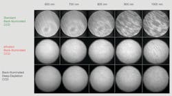
Finally, since the new technology is based on a standard back-illuminated architecture, it has similar dark current (in both cases, as much as 100 times lower than that of back-illuminated deep-depletion CCDs). In other words, deep-depletion CCDs require deeper cooling to achieve similar dark-noise performance as that of eXcelon detectors. This is an important consideration, especially in spectroscopy, where the signal is integrated over many minutes and binned over several rows. Similar gains in performance can be realized using eXcelon back-illuminated EMCCDs in low-noise camera designs.
Ways to further improve camera sensitivity
While sensor technology is an important factor in camera-system sensitivity and signal-to-noise ratio for a given experiment, other factors such as low-noise camera electronics and optical window throughput are also important.
To maximize light throughput, we use a single-window vacuum design with a brazed metal-to-glass interface. As a result, the vacuum window is the only optical surface encountered by incident photons before they reach the CCD or EMCCD detection surface. Although the design is the best available, each uncoated optical surface of the vacuum window can still have 3% to 4% transmission loss, for a total loss of 6% to 8%. For light-starved imaging applications, this loss can result in a significant reduction of signal-to-noise ratio. Moreover, any light reflected inside the system can lead to glare and fringing, especially when used with coherent illumination. The solution is to apply antireflective coatings on the window, which reduce total losses to below 0.5% to 1%. For applications using extremely coherent light sources, a wedge-shaped window may also be required to eliminate residual glare and fringing.
High sensitivity over a broad wavelength range, as well as lower etaloning than standard back-illuminated sensor technology, make these sensors well-suited for both science and industrial use. Applications of the new technology include astronomical imaging, Bose-Einstein condensate imaging, single-molecule fluorescence, solar cell inspection, and Raman spectroscopy, to name a few.
REFERENCE
- N.I. Hammer et al., J. Phys. Chem. B, 110, 14167 (2006).
About the Author

Ravi Guntupalli
Product Manager
Ravi Guntupalli is a product manager at Princeton Instruments, a leading provider of scientific grade CCD, ICCD, EMCCD and InGaAs based cameras and spectrographs for ultra low light imaging and spectroscopy applications. With over 14 years of experience in the field of low light imaging technonologies, Ravi has been working with researchers worldwide who are applying these technologies across life and physical sciences.