INFRARED IMAGING: Infrared arrays see temperature gradients
To the unaided human eye, most objects are visible by the reflection of light from the sun or from a man-made source. We are, therefore, unable to detect their presence when such a source is absent, that is, when it is dark. In most cases, reflectivity is independent of temperature up to the boiling point of water so that contact methods (touch, for example) provide our only means for detecting temperature gradients. As we move into the mid-infrared (IR) region of the spectrum, this situation changes dramatically with all objects acting as IR 'light bulbs' whose brightness and spectrum are determined, to first order, by temperature. Thus, an IR-sensitive imaging system can see objects without external illumination in addition to detecting spatial temperature variations of less that 1/10 K.
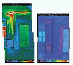
For these reasons, imaging systems that operate in the mid- and long-wavelength IR atmospheric windows are useful for a wide range of research applications in addition to more practical tasks, including nondestructive testing, failure prediction, tactical imaging, surveillance, and mapping. For example, law-enforcement agencies routinely use IR-sensitive cameras for drug surveillance because the high-intensity used to grow illegal plants in an indoor environment give off a significant amount of heat. Venting of this excess heat to the environment usually modifies the IR signature of a building in a way that is easily detected with a hand-held IR camera.
In many industrial environments, excess heating of a part is often a prelude to failure. Infrared imaging systems can be used to visualize hot spots, thereby identifying candidates for more-detailed inspection and/or replacement.
Depending on the application, a wide range of infrared imaging technologies are currently available. Cost, ease of use, acquisition speed, spectral response, and sensitivity must all be taken into consideration when selecting a system, although cost and ease of use are usually the most important for nonmilitary applications. As a result, the largest, most-sensitive arrays are typically purchased by government and scientific customers, with the more-economical systems finding their way into the commercial sector.
Planck's Law
It is useful to look briefly at the transmission of IR light by the atmosphere and the relationship between the temperature and emission spectrum of an ideal emitter (blackbody source). Qualitatively, the spectral region between 1 and 14 µm is divided into three regions that are separated by strong atmospheric absorptions. Short-wavelength infrared radiation (SWIR) lies in the most energetic window, stretching from the upper edge of the visible spectrum around 850 nm to a region of strong attenuation near 3 µm. The mid-wavelength infrared (MWIR) region lies between 3 and 6 µm, with the long-wavelength infrared (LWIR) window stretching from the upper edge of the broad 6-µm absorption to an upper limit of 14 µm. Detector arrays are usually optimized for efficient operation in a single band, the selection of which is application-dependent.
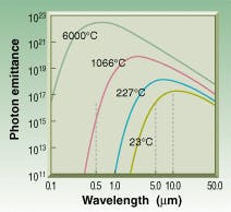
In the ideal case, the spectral emission from real objects can be approximated by that of a blackbody radiation source having an emission spectrum described mathematically by Planck's Law. This relationship states that the number of photons emitted at a particular wavelength increases with temperature, while the peak of the spectral-emission function moves to shorter wavelengths (see Fig. 1). For example, we find that a blackbody source must be heated to 1000°C for the number of photons emitted at 500 nm to approximately equal the room-temperature emission at 5000 nm (5 µm). The peak of the 273 K emission curve occurs near 10 µm, where the emission is approximately 10 times greater than the 5-µm value.For the mid- and long-wavelength regions, Planck's Law also indicates that the emission is a sensitive function of temperature. As a result, commercial cameras operating in these bands are capable of routinely detecting temperature differences as small as 0.070 K.
For many applications, the selection of a spectral region is determined by the available hardware. For example, thermal imaging can be readily carried out in both the MWIR and LWIR regions so that the operational characteristics and cost of an IR imaging system becomes the determinant. Defense applications are much less cost-sensitive and often require the highest sensitivity and resolution in multiple transmission windows.
PtSi provides MWIR resolution
Although several different array types have been developed for imaging applications in the MWIR region of the spectrum, platinum silicide (PtSi) devices currently dominate the commercial market. Based on a monolithic silicon fabrication technology, these devices have the multiple advantages of fabrication ease (which translates into lower cost), spatially uniform response, and good sensitivity. Currently, a number of manufacturers offer PtSi arrays in pixel sizes ranging from 256 × 256 to 1024 × 1024, with larger sizes expected in the near future. Alternative detector technologies (HgCdTe and InGaAs, for example) have significantly higher MWIR sensitivities but are much harder to manufacture and are significantly more expensive.
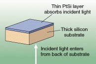
Platinum silicide devices are part of a unique class of detectors that consist of a comparatively thick p-type silicon substrate and a thin layer of metal on one side (see Fig. 2). Infrared radiation enters through the substrate (backside illumination) and is absorbed by the PtSi, generating a positively charged hole. If the IR radiation is energetic enough (wavelength below cutoff), an electron from the semiconductor material can pass through the potential barrier that exists between the PtSi layer and the substrate. This electron then combines with the hole in the PtSi layer, thereby generating a photon (internal photoemission). This effect is also observed with other metal silicides including iridium, palladium, and nickel, each with a different cutoff wavelength determined by the height of the potential barrier between the metal silicide and the substrate. Platinum silicide has a cutoff wavelength of 5.5 µm—well-matched to the upper edge of the MWIR transmission window.In a typical array, charge is transferred from the PtSi detector element to readout elements that are physically adjacent to it on the silicon substrate. As a result, these arrays are electronically similar to those of a visible CCD (see Laser Focus World, Jan. 1999, p. 117). From a manufacturing standpoint, the use of monolithic silicon technology is a major advantage with respect to other IR detector types that require gates to be formed in less familiar materials or the use of hybrid designs in which the detector elements are formed on a different substrate from the readout gates.
At wavelengths below cutoff, electrons from the silicon penetrate the potential barrier that exists between the PtSi layer and the substrate, combining with the holes in a process known as internal photoemission. Efficient operation of a PtSi array requires that it be cooled to liquid-nitrogen temperature. Fortunately, compact Stirling coolers can be used to accomplish this task in a package that is similar in size and weight to a large video camera. These coolers are quiet and relatively compact, their primary drawback being a life cycle that is significantly shorter than the arrays they cool.
HgCdTe dominates LWIR region
Mercury cadmium telluride (HgCdTe) is a unique intrinsic (undoped) semiconductor whose bandgap can be compositionally tuned over a wide energy range. As a result, materials having different mercury-to-cadmium ratios can be used to detect radiation in all three IR transmission windows. Useful in both photovoltaic (absorption of light produces a voltage) and photoconductive (light produces a change in conductivity) modes, its properties are most advantageous in the LWIR region where PtSi cannot be used.
In this region, HgCdTe has the dual advantages of reduced cooling requirements with respect to detectors that are based on doped semiconductor materials and a high absorption coefficient. Intrinsic materials do not have low-lying impurity energy levels that are characteristic of doped materials, and higher temperatures are needed for thermally generated carriers to reach the conduction band. As a result, HgCdTe arrays that are designed to operate in the 8- to 12-µm range can run at 77 K, while Si:As detectors that are sensitive from 2 to 28 µm must operate below 10 K.
One of the best developed IR materials, HgCdTe has been heavily used for defense applications in the LWIR region since the early 1970s. Despite its wide use, the material is plagued by compositional variations that are difficult to control during growth. Spatial variations in the mercury-to-cadmium ratio across a boule alter the cutoff wavelength and sensitivity and degrade the performance of detector arrays. In practice, uniform regions of appropriate composition are selected from as-grown material on the basis of an x-ray analysis of the crystallographic structure. These variations are less important at shorter wavelengths, where the spectral sensitivity (cutoff wavelength) of the material is less dependent on composition.
Although HgCdTe is significantly more sensitive than PtSi in the MWIR band, its use has been primarily confined to military applications for which a significantly higher cost can be tolerated. In the commercial sector, the sensitivity of PtSi is adequate for most applications, and the $20,000 cost of a basic camera makes the technology highly attractive in many applications.
Room-temperature alternatives
While PtSi and semiconductor detectors can be used to fabricate detector arrays with reasonably high sensitivity and resolution, pyroelectric and microbolometer arrays offer room-temperature operation at reduced sensitivity. Available as single-element detectors for many years, these alternatives are referred to as thermal detectors because they use the rise in temperature after the absorption of light as a measure of incident power. In the case of a bolometer, a change in temperature results in a change in detector resistance that can be measured using an external circuit. In the case of a pyroelectric detector, the capacitance of a ferroelectric element is changed. Both detector types have a broad, flat spectral response determined by the absorptivity of the detector surface.
Silicon microbolometer arrays are sensitive to LWIR radiation, are comparatively easy to manufacture, and are free from the spatial uniformity issues that plague HgCdTe. More important, they can operate at room temperature, eliminating the need for cryogenic cooling. Because the photon-emission rate is typically higher in the long-wavelength region, microbolometer arrays operating in this band can image temperature gradients as small as 0.1 K—a value that is comparable to that of PtSi-based cameras operating at shorter wavelengths.
At the present time, PtSi arrays offer higher resolution than microbolometers. However, the fact that the thermal-detector technology can operate without coolers is a strong advantage for certain users. In law-enforcement surveillance work, where thermal imagery is used for a variety of tasks, municipalities and county governments often opt for uncooled cameras while state and federal agencies buy PtSi-based devices. Although the microbolometer-based systems have lower resolution, their performance is more than adequate for most tasks. A slightly lower cost coupled with an extended operating life (no Stirling cooler to go bad) are important advantages for budget-limited organizations.
Ultimately, progress in the development of room-temperature arrays should result in significant cost reductions and improved resolution. As progress is made, one can expect these systems to be preferred in commercial applications where ease of use and lifetime are important concerns. Electronic arrays such as PtSi and HgCdTe should still be used in applications for which high resolution and sensitivity are required, although the cryogenically cooled operation of these devices will continue to present cost and lifetime issues. Overall, the continued development of infrared imaging systems should ultimately make infrared camera systems as easy to use as the visible CCD-array-based devices available today.
ACKNOWLEDGMENT
The author thanks the education department of SPIE for providing copies of notes from courses entitled "Infrared Photodetectors" and "Imaging Detectors." Course dates and fees can be obtained from SPIE, POB 10, Bellingham,WA 98277-0010 or on the Web: www.spie.org.


