2014 VLSI Symposia to delve into CMOS silicon-photonics technology
The upcoming 2014 Symposia on VLSI Technology & Circuits (June 9 to 13, 2014; Honolulu, HI) will cover leading-edge developments on semiconductor technology and circuits—mostly electronics, but some photonics too. The two programs offered are "Technology" and "Circuits," both of which offer papers on silicon photonics based on the economical CMOS manufacturing process.
Although the full papers won't be released until June 8, the abstracts offer interesting tidbits on the technology that will be described in full at the Symposia.
Monolithically integrated CMOS optical link
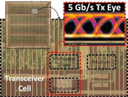
Of particular note is a highlighted paper from a team led by Micron Technology (Boise, ID), describing the first monolithic silicon-photonics-on-bulk-CMOS process flow to connect distant distributed memory devices (Paper T21.1, “Integration of Silicon Photonics in Bulk CMOS,” R. Meade et al., Micron, MIT, U. of Colorado, and UC Berkeley).
The Micron device includes deep-trench isolation, polysilicon waveguides, grating couplers, filters, modulators, and detectors. Fully functional on-chip CMOS enables transmit/receive operation while minimizing interconnect parasitics. With the addition of an external 1280 nm light source, a fully functional optical link (5 Gbit/s with 2.8 pJ/bit), capable of WDM (wavelength division multiplexing), has been demonstrated. In addition to the polysilicon resonant detector used in the link, a monolithically integrated silicon-germanium (SiGe)-based photodetector using selective epitaxial growth was also developed.
From the abstract: "Other research groups have published on SOI devices or 'stand-alone' silicon photonics (i.e. not monolithically integrated). This paper is different in that, for the first time, a working optical link has been demonstrated on an economically feasible (specifically for memory) CMOS platform. Today, 3D integration is a major industry focus in part due to the power and performance requirements of chip-to- chip I/O. While 3D integration is important, this research shows a clear alternative path that has significant benefits."
The result is a monolithically integrated optical chip-to-chip link that transmits 5 Gbit/s over distances up to 5 m long (via fiber link).
Other photonics-related presentations
A group from National University of Singapore and Nanyang Technological University will present "Germanium-Tin on Silicon Avalanche Photodiode for Short-Wave Infrared Imaging," in which a monolithic, CMOS-compatible germanium-tin on silicon (Ge1-xSnx/Si) avalanche photodiode (APD) for short-wave infrared (SWIR) imaging is reported that has a lower thermal sensitivity than conventional III-V-based aAPDs.
Researchers from Taiwan Semiconductor Manufacturing Company will present "Advanced 1.1 μm Pixel CMOS Image Sensor with 3D Stacked Architecture," in which they describe their 1.1-μm-pixel backside-illuminated CMOS image sensor with a 3D stacked architecture. The carrier wafer in conventional BSI is replaced by an ASIC wafer, which simplifies fabrication and improves dark performance.
A team from MIT and the University of Colorado, Boulder (many members of whom also worked on the Micron Technology device) will present "A Monolithically-Integrated Optical Transmitter and Receiver in a Zero-Change 45 nm SOI Process." Here, according to the abstract, "an optical transmitter and receiver with monolithically-integrated photonic devices and circuits are demonstrated together for the first time in a commercial 45 nm SOI [silicon-on-insulator] process, without any process changes. The transmitter features an interleaved-junction carrier-depletion ring modulator and operates at 3.5 Gbit/s with an 8 dB extinction ratio and combined circuit and device energy cost of 70 fJ/bit. The optical receiver connects to an integrated SiGe detector designed for 1180 nm wavelength and performs at 2.5 Gbit/s with 15 μA sensitivity and energy cost of 220 fJ/bit."
For more info, see http://www.vlsisymposium.org/
About the Author
John Wallace
Senior Technical Editor (1998-2022)
John Wallace was with Laser Focus World for nearly 25 years, retiring in late June 2022. He obtained a bachelor's degree in mechanical engineering and physics at Rutgers University and a master's in optical engineering at the University of Rochester. Before becoming an editor, John worked as an engineer at RCA, Exxon, Eastman Kodak, and GCA Corporation.

