Fujifilm and Panasonic create organic CMOS sensor with 88 dB dynamic range
Tokyo and Osaka, Japan--Fujifilm Corp. and Panasonic Corp. have developed organic CMOS image-sensor technology that has a large dynamic range of 88 dB, preventing simultaneous overexposure in bright image areas and underexposure in dark areas.
The details of the technology were announced at the 2013 Symposia on VLSI Technology and Circuits (June 11 to 14, 2013; Kyoto, Japan; lecture numbers T2-4 and C2-3). The titles of T2-4 and C2-3 were "Thin Organic Photoconductive Film Image Sensors with Extremely High Saturation of 8500 electrons/μm2" and "An Ultra-low Noise Photoconductive Film Image Sensor With a High-speed Column Feedback Amplifier Noise Canceller," respectively.
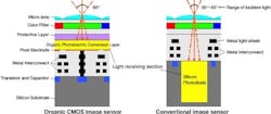
Fujifilm developed an organic photoconductive film (OPF) with a high optical-absorption coefficient instead of the usual silicon (Si) photodiode for the light-receiving portion of the sensor.
The new device, which is the result of combining Fujifilm's OPF technology and Panasonic's semiconductor device technologies, has—in addition to the 88 dB dynamic range—a 1.2-times-higher sensitivity and high sensitivity over a large range of incident light angles, Fujifilm and Panasonic plan to use the organic CMOS image sensor technology for security cameras, automotive cameras, mobile devices, digital cameras, and so on.
0.5-μm-thick OPF
The thickness of the OPF is 0.5 μm, which is several times thinner than that of a Si photodiode; this allows a signal saturation value four times higher than those of conventional image sensors.
For conventional image sensors, it is necessary to form metal wires for each pixel and a light-blocking film to prevent light from entering areas other than the photodiode area, limiting the area of the light-receiving part. Here, however, the OPF covers the whole surface, improving sensitivity. In addition, conventional Si photodiodes require a thickness of about 3 μm in the depth direction, limiting their incident light angles to about 30-40°. In the new device, an incident light angle of 60° is allowed by the thin OPF.
Fujifilm developed a process technology to form an inorganic thin film that protects the OPF, preventing moisture and oxygen from entering the OPF. The result is an organic CMOS sensor that can pass temperature, moisture, voltage, and light stress tests.
Source: http://techon.nikkeibp.co.jp/english/NEWS_EN/20130612/287440/?P=2
About the Author

John Wallace
Senior Technical Editor (1998-2022)
John Wallace was with Laser Focus World for nearly 25 years, retiring in late June 2022. He obtained a bachelor's degree in mechanical engineering and physics at Rutgers University and a master's in optical engineering at the University of Rochester. Before becoming an editor, John worked as an engineer at RCA, Exxon, Eastman Kodak, and GCA Corporation.