Cambridge, MA--Researchers from the Massachusetts Institute of Technology (MIT) and five other institutions have developed a laser-based gold-doping procedure that enables silicon to exhibit a broad infrared response at room temperature. Silicon, which forms the basis of most semiconductor and solar-cell technology, normally lets most infrared light pass right through. But the new method could change that, making silicon useful as an imaging array for security systems or as a better solar cell that absorbs infrared energy.
The new gold-infused-silicon approach is described in a paper published in the journal Nature Communications by MIT graduate student Jonathan Mailoa, associate professor of mechanical engineering Tonio Buonassisi, and 11 others. "Silicon usually has very little interaction with infrared light," Buonassisi says. Various treatments of silicon can mitigate this behavior, usually by creating a waveguide with structural defects or doping it with certain other elements. The problem is that most such methods have significant negative effects on silicon's electrical performance; only work at very low temperatures; or only make silicon responsive to a very narrow band of infrared wavelengths.
The new system works at room temperature and provides a broad infrared response, Buonassisi says. It incorporates atoms of gold into the surface of silicon's crystal structure in a way that maintains the material's original structure. Additionally, it has the advantage of using silicon, a common semiconductor that is relatively low-cost, easy to process, and abundant.
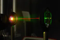
The approach works by implanting gold into the top hundred nanometers of silicon and then using a laser to melt the surface for a few nanoseconds. The silicon atoms recrystallize into a near-perfect lattice, and the gold atoms don't have time to escape before getting trapped in the lattice. In fact, the material contains about 1% gold, an amount more than 100 times greater than silicon's solubility limit. This solution produces a layer of silicon supersaturated with gold atoms.
"It's still a silicon crystal, but it has an enormous amount of gold near the surface," Buonassisi says. While others have tried similar methods with materials other than gold, the MIT team's work is the first clear demonstration that the technique can work with gold as the added material, he says. "It's a big milestone, it shows you can do this," Mailoa says. "This is especially attractive because we can show broadband infrared response in silicon at room temperature." While this is early-stage work, for some specialized purposes—such as a system for adjusting infrared laser alignment—it might be useful relatively quickly.
This use of gold was a surprise: Usually gold is incompatible with anything involving silicon, Buonassisi says. Even the tiniest particle of it can destroy the usefulness of a silicon microchip—so much so that in many chip-manufacturing facilities, the wearing of gold jewelry is strictly prohibited. "It's one of the most dangerous impurities in silicon," he says. But at the very high concentrations achieved by laser doping, Buonassisi says, gold can have a net positive optoelectronic impact when infrared light shines on the device.
While this approach might lead to infrared imaging systems, Buonassisi says, its efficiency is probably too low for use in silicon solar cells. However, this laser processing method might be applicable to different materials that would be useful for making solar cells, he says.
The research was funded by the U.S. Army Research Office, the National Science Foundation, the U.S. Department of Energy, and the MIT-KFUPM Center for Clean Water and Energy, a joint project of MIT and the King Fahd University of Petroleum and Mining.
SOURCE: MIT; http://web.mit.edu/newsoffice/2013/making-silicon-devices-responsive-to-infrared-light-0102.html
About the Author

Gail Overton
Senior Editor (2004-2020)
Gail has more than 30 years of engineering, marketing, product management, and editorial experience in the photonics and optical communications industry. Before joining the staff at Laser Focus World in 2004, she held many product management and product marketing roles in the fiber-optics industry, most notably at Hughes (El Segundo, CA), GTE Labs (Waltham, MA), Corning (Corning, NY), Photon Kinetics (Beaverton, OR), and Newport Corporation (Irvine, CA). During her marketing career, Gail published articles in WDM Solutions and Sensors magazine and traveled internationally to conduct product and sales training. Gail received her BS degree in physics, with an emphasis in optics, from San Diego State University in San Diego, CA in May 1986.
