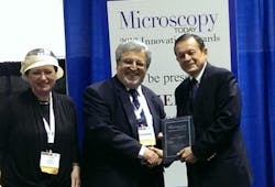
Nanonics wins microscopy award for integrated AFM/SEM/FIB instrument
Jerusalem, Israel--Integrated microscopy imaging company Nanonics is proud to announce that our triple beam integrated atomic force microscopy/scanning electron microscope/focused ion beam (AFM/SEM/FIB) system, the Nanonics 3TB4000, was judged one of the ten best microscopy innovations in 2013 and is the recipient of the prestigious 2013 Microscopy Today Innovation Award (http://www.microscopy-today.com/jsp/awards/awards.jsf). The 3TB4000 provides the ultimate 3D nanoscale characterization capability through a revolutionary innovation of open architecture that provides open access to the SEM/FIB beams without any obstruction or interference to the injectors, detectors, or beam lines.
With the 3TB4000, the SEM, FIB, and AFM can now be used to provide complimentary information in order to provide a complete nanocharacterization of material by taking advantage of the functional and high resolution 3D capabilities of AFM, the large field of view and rapid scanning of the SEM, and the fabrication/material removal capability of the FIB. Applications demonstrating this powerful new capability have been shown in diverse areas including sidewall imaging in semiconductors, locating and measuring optical properties of individual metal oxide nanowires or mechanical properties of surface features, and assessing AFM probes in situ while imaging.
Nanonics products include near-field scanning optical microscope (NSOM) imaging instruments with cantilevered NSOM probes, dual tip/sample scanning AFM systems, and the first ever NSOM/AFM cryogenic systems, optical tweezers , Raman/AFM, multiprobe AFM, and SEM/AFM systems.
SOURCE: Nanonics; http://www.nanonics.co.il/company/news/nanonics-triple-beam-afm-sem-fib-system-is-one-of-the-ten-best-microscopy-innovations-in-2013.html
About the Author

Gail Overton
Senior Editor (2004-2020)
Gail has more than 30 years of engineering, marketing, product management, and editorial experience in the photonics and optical communications industry. Before joining the staff at Laser Focus World in 2004, she held many product management and product marketing roles in the fiber-optics industry, most notably at Hughes (El Segundo, CA), GTE Labs (Waltham, MA), Corning (Corning, NY), Photon Kinetics (Beaverton, OR), and Newport Corporation (Irvine, CA). During her marketing career, Gail published articles in WDM Solutions and Sensors magazine and traveled internationally to conduct product and sales training. Gail received her BS degree in physics, with an emphasis in optics, from San Diego State University in San Diego, CA in May 1986.
