Vanadium-sapphire device from Harvard boasts nearly 100% IR absorption on demand
Cambridge, MA--A new optical surface created by Federico Capasso and his group at the Harvard School of Engineering and Applied Sciences (SEAS) in collaboration with scientists at the University of California San Diego can absorb 99.75% of infrared (IR) light that strikes it. When thermally activated, it appears black to IR cameras.
Ultrathin and tunable
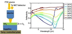
Composed of just a 180-nm-thick layer of vanadium dioxide (VO2) on top of a sheet of sapphire, the device reacts to temperature changes by reflecting dramatically more or less IR light. Announced today in the journal Applied Physics Letters and featured on its cover, this perfect absorber is ultrathin, tunable, and exceptionally well-suited for use in a range of IR optical devices.
Perfect absorbers have been created many times before, but not with such versatile properties. In a Fabry-Pérot cavity, for instance, two mirrors sandwich an absorbing material, and light simply reflects light back and forth until it's absorbed. Other devices incorporate surfaces with nanoscale metallic patterns that trap and eventually absorb the light.
"Our structure uses a highly unusual approach, with better results," says Capasso, the principal investigator. "We exploit a kind of naturally disordered metamaterial, along with thin-film interference effects, to achieve one of the highest absorption rates we've ever seen. Yet our perfect absorber is structurally simpler than anything tried before, which is important for many device applications."
Sudden transition
Vanadium dioxide is normally an insulating material. Take it from room temperature up to about 68°C, however, and it undergoes a dramatic transition: the crystal rearranges itself as the temperature approaches a critical value. Metallic islands appear as specks, scattered throughout the material, with more and more appearing until it has become uniformly metallic.
“Right near this insulator-to-metal transition, you have a very interesting mixed medium, made up of both insulating and metallic phases,” says coauthor Shriram Ramanathan, who synthesized the thin film. “It’s a very complex and rich microstructure in terms of its electronic properties, and it has very unusual optical properties.” Those properties, when manipulated correctly, happen to be ideal for IR absorption.
And the underlying sapphire substrate, although usually transparent, has a crystal structure that actually makes it opaque and reflective, like a metal, to a narrow subset of IR wavelengths. The result is a combination of materials that internally reflects and absorbs incident IR light.
"Both of these materials have lots of optical losses, and we've demonstrated that when light reflects between lossy materials, instead of transparent or highly reflective ones, you get strange interface reflections," explains lead author Mikhail Kats. "When you combine all of those resulting waves, you can coax them to destructively interfere and completely cancel out. The net effect is that a film one hundred times thinner than the wavelength of the incident light can create perfect absorption."
Very pure VO2 neededOne challenge is learning how to fabricate pure-enough samples of the VO2. “Vanadium oxide can exist in many oxidation states, and only if you have VO2 does it go through a metal-insulator transition close to room temperature,” Ramanathan says. “We have developed several techniques in our lab to allow exquisite compositional and structural control, almost at the atomic scale, to grow such complex films. The resulting phase purity allows us to see these remarkable properties, which otherwise would be very difficult to observe.”
Possible applications include bolometers with tunable absorption, spectroscopy devices, tunable filters, thermal emitters, radiation detectors, and equipment for energy harvesting. Harvard’s Office of Technology Development has filed patent applications on the novel invention and is actively pursuing licensing and commercialization opportunities.
About the Author
John Wallace
Senior Technical Editor (1998-2022)
John Wallace was with Laser Focus World for nearly 25 years, retiring in late June 2022. He obtained a bachelor's degree in mechanical engineering and physics at Rutgers University and a master's in optical engineering at the University of Rochester. Before becoming an editor, John worked as an engineer at RCA, Exxon, Eastman Kodak, and GCA Corporation.

