Millimeter-long GaN nanowires grow horizontally
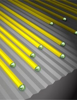
Rehovot, Israel--Weizmann Institute professor Ernesto Joselevich has found a way to grow semiconductor nanowires horizontally (not vertically as is typical) on a surface, enabling for the first time the much-needed guidance to produce relatively long, orderly, aligned structures. Since semiconductors with controlled structures are at the core of the most advanced technologies, these new semiconductor nanostructures should offer enhanced electronic and optical properties useful for a wide range of applications including LEDs, lasers, information storage media, transistors, computers, photovoltaics, and more.
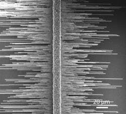
Their results, recently published in Science (http://www.sciencemag.org/content/333/6045/1003.full?sid=93f889c5-0110-4e80-8810-2d518673ff79) show that surface steps and grooves have a strong guiding effect, coaxing the nanowires to grow horizontally along their edges or within the grooves and producing well-aligned, millimeter-long nanowire arrays. In contrast, current methods of assembling nanowires horizontally on smooth surfaces result in disorderly nanowires only micrometers in length with subpar properties.
Although the mechanisms that create the long nanowires are still not well understood, the team has managed the synthesis and assembly of well-structured nanowires with unique properties suitable for a wide range of applications by simply getting them “into the groove.”
SOURCE: Weizmann Institute of Science; http://wis-wander.weizmann.ac.il/nanowires-get-into-the-groove