SILICON PHOTONICS: Nanopillar lasers are grown on silicon
Successful growth of nanopillar III-V lasers on silicon (Si) by Connie Chang-Hasnain's group at the University of California at Berkeley (Berkeley, CA) has opened a new approach to integrating photonics with electronic circuits. The fabrication technique overcomes temperature incompatibilities and lattice mismatches that had previously blocked the direct growth of lasers on Si chips.
Integrating lasers with Si electronics has become a holy grail because of its importance for the future of high-performance computing. As described in this month's Photonic Frontiers (see page 57), photons can transmit high-speed signals faster than electrons between the multiple processing cores fabricated on chips, as well as between chips on circuit boards. Silicon can supply waveguides and detectors for optical links, but it lacks the direct bandgap needed to make good diode lasers. To fill that need, developers have focused on combining III-V diode lasers with Si.
In another approach, Intel Corp. (Santa Clara, CA) and the University of California at Santa Barbara (Santa Barbara, CA) have developed a hybrid laser by bonding an indium phosphide (InP) chip containing a diode junction to a waveguide in a Si chip. Carriers recombine at the InP junction, generating light that is coupled into the Si waveguide and can be routed to a detector.
Chang-Hasnain's group has focused instead on growing gallium arsenide nanopillar emitters directly on Si. Last year they reported growing indium gallium arsenide (InGaAs) LEDs on Si; now they report fabricating a nanopillar InGaAs laser.1, 2
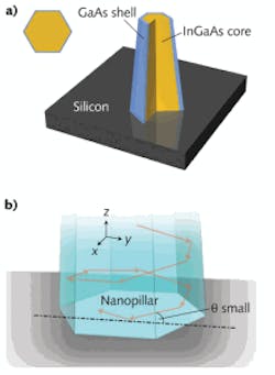
Resonator with helical path
The hexagonal InGaAs pillars are about 600 μm wide at the base and taper toward the top at an angle of about 5°; a thin GaAs layer passivates the device. The demonstration lasers were optically pumped by illuminating their tops with 120 fs modelocked pulses from an external titanium:sapphire laser emitting at 750 nm. The tapered nanopillar formed a novel resonator, with the 950 nm laser emission following a helical path reflected around the pillar by successive facets and directed downward toward the larger base, where the light coupled into the Si (see figure).
The Berkeley experiment shows that lasers can be grown on Si, a crucial step because lasers were the missing element needed for optical data links. But much work remains. One challenge is electrically pumping the tiny laser as needed for a practical photonic interconnection on a chip, notes lead author Roger Chen, but he adds that his group has already demonstrated nanopillar LEDs with internal junctions.
Light transmission in Si poses another challenge: the 950 nm output of the InGaAs lasers is strongly absorbed. Silicon transmits well beyond 1100 nm at the longer wavelengths of phosphide-based lasers; the growth techniques can be modified to include more indium to extend to these longer wavelengths, as Chang-Hasnain's group reported earlier.3
So far, the Berkeley researchers have grown lasers only on raw Si, but practical applications will require fabrication on chips with CMOS circuits already in place on the Si. They expect that will be possible because their process grows nanopillars at about 400°C, a temperature which is well below those normally used for growing III-V structures, and which is compatible with CMOS devices.
Much remains to be demonstrated, but Chen and Chang-Hasnain are optimistic. Grown directly on Si, nanopillar lasers "offer tiny footprints and scalability, and are thus particularly suited to high-density optoelectronics," they write in Nature Photonics. They predict that future electrically pumped p-i-n versions promise "a powerful marriage between photonic and electronic circuits."
REFERENCES
1. L.C. Chuang, "InGaAs QW nanopillar light emitting diodes monolithically grown on a Si substrate." 2010 Conference on Lasers and Electro-Optics, paper CMFF6 (OSA, 2010).
2. R. Chen et al., Nature Photon.; doi: 10.1038/NPHOTON.2010.315.
3. M. Moewe et al., Opt. Exp., 17, 7831 (2009).
About the Author

Jeff Hecht
Contributing Editor
Jeff Hecht is a regular contributing editor to Laser Focus World and has been covering the laser industry for 35 years. A prolific book author, Jeff's published works include “Understanding Fiber Optics,” “Understanding Lasers,” “The Laser Guidebook,” and “Beam Weapons: The Next Arms Race.” He also has written books on the histories of lasers and fiber optics, including “City of Light: The Story of Fiber Optics,” and “Beam: The Race to Make the Laser.” Find out more at jeffhecht.com.