Sophisticated optical instrumentation facilitates advanced bioimaging, and high-performance optical filtering improves fluorescence detection systems. Because proper optical filtering boosts throughput and enables wide-scale blocking, it solves problems like increasing the sensitivity of a system to detect infinitesimally small fluorescent signals emitted from biological samples. Too much light can lead to overexposure at the sensor, thus masking the signal—the filter helps to remove unwanted light so that the fluorescence response can be identified and measured. In fact, filters are arguably the most important element defining system performance for fluorescence detection. And thanks to manufacturing innovation, they can do so at competitive price points. Let's take a look at some important concepts in optical filtering and how they can improve outcomes in biomedical research.
Bandpass filters
Bandpass filters transmit light at a specific wavelength, or over some wavelength band, while blocking the adjacent spectrum on either side. They are important for life sciences because they allow separation—in some cases with sub-nanometer level accuracy—of critical vs. unwanted light in the final image. Thin-film, hard-coated bandpass filters offer higher light throughput compared to soft-coating alternatives. This, combined with steeper transitions to high out-of-band optical density (OD) blocking, enables enhanced signal-to-noise ratios (S/N). This can have a dramatic impact on outcomes for applications like laser scanning fluorescence confocal microscopy, for instance, where the S/N is a key consideration and ultimately dictates the achievable contrast in the final image quality.
There are two fundamental approaches to designing a bandpass. Cavity filters rely on stacked Fabry-Perot resonant cavities, while the other method uses individual longwave-pass (LWP) and shortwave-pass (SWP) filters, which are combined to form both edges of the bandpass. Cavity filters are symmetric in shape while LWP and SWP designs can be made asymmetric, which can help to lower cost in certain situations.
Both types are paired with blocking elements, which determine the level of light attenuation outside the passband, or region of high transmission. These blocking elements can be dielectric blockers such as additional SWP and LWP filters, or non-dielectric elements such as light-absorbing colored glass. The latter are subject to cost, autofluorescence (AF) concerns, and reliability issues. In general, thin-film blocking elements are simple in construction and design, but can add substantial cost if overspecified. For fluorescence applications, blocking levels of 5 to 6 OD average, out-of-band, are recommended. Special consideration should be given to crossover bands—that is, where an excitation filter cuts off and an emission filter cuts on. Blocking coverage should be greater at these points, depending on the application and system implementation of the filter. Improper blocking coverage in this region may produce undesirable light leakage effects in the system.
The "squareness" of a signal is also important because it enables a steeper transition between high %T in the passband to high OD blocking. The squarer the filter shape becomes, the more vertical the edges of the bandpass (or edge) filter. This might be critical in a Raman spectroscopy instrument, for instance, where the excitation and emission modes for the fluorophore of interest are very close in wavelength space. The laser line filter needs to have a steep and well-defined cut-off edge to modulate the laser source and, conversely, the laser blocking filter (often a Raman longpass) needs to have a steep cut-on edge to completely block the light from the laser. Designing bandpass filters to generate steeper signal slopes (that is, to improve squareness) is a relatively simple matter of adding more cavities to the filter design (see Fig. 1a). Improving the slope on the LWP and SWP approaches is much the same, although in this case the designer adds more layers.
However, adding cavities poses challenges for control of the deposition process, and invariably introduces undesirable ripple and loss to the passband. For life scientists, this can mean false color or contrast reduction in the images they are collecting. A novel optical thickness monitoring approach enables an increase in optical cavity count to as many as 20 while maintaining low passband ripple-well in excess of industry limits of approximately 10 cavities. This system works by continually measuring the filter function and compensating for thickness errors associated with prior layers. Figure 1b shows four coating runs of the same design overlaid for two different high-cavity-count filters designed as emission filters. This novel monitoring approach facilitates more challenging designs to be manufactured with relative ease and-most importantly—with high repeatability. For technologists, this grants the flexibility to specify their filters to meet high-performance system requirements, with assurance that the filter can be produced with accuracy for high volumes.
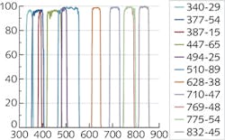
Because light wavelengths that are effective for interacting with tissue generally fall between 340 and 900 nm, optical filters for life sciences follow suit. Figure 2 shows typical transmission response, or %T, as a function of the wavelength spectrum for a variety of common filter wavelengths and bandwidths. These filters are fully blocked, meaning all wavelengths outside the passband are rejected, to 6 OD or greater to ensure signal-to-noise (S/N) ratios. OD is the log (base 10) of transmittance (T) and a commonly used term to describe the rejection level of filter.Out-of-band blocking
Fluorescence detection filters are characterized in terms of blocking level, particularly with respect to the overlap of the excitation filter. As introduced above, there is a crossover point in wavelength space where the excitation response declines and the emission response inclines. For the excitation filter, it's critical to block this point and everything to the right of this point (extending past the emission passband). Especially for the emission filter, it's necessary to block this overlap point and wavelengths to the left (extending past the start of the excitation passband). The excitation signal needs to be completely blocked in the emitter; otherwise, the much brighter excitation light overwhelms the weaker emitted fluorescence light from the specimen. Blocking can be thought of as the denominator in the optical S/N calculation. Figure 1c shows blocking levels of the emission filter depicted in Figure 1b. This filter has all the bandpass and blocking layers on a single side of the substrate, which improves transmission and reduces cost. An anti-reflection (AR) coating on the back of the substrate improves transmission at nominal extra cost.
The measurement of blocking levels is a difficult subject and generally limited to noise floors of the spectrophotometer of between 6 and 7 OD. When measuring OD, you're essentially trying to detect the absence of light—so a very sensitive detector is needed to accurately detect photons at this level. Most spectrophotometers are limited in this capability because detector technology cannot accommodate the dynamic range necessary to measure a filter with very high transmission in one wavelength region and practically no light in another. When measuring OD >5.5, even the most challenging considerations to quantify, like stray light and electronic noise, need to be accounted for to address the noise floor issue.
Multi-bandpass filters
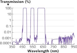
The latest bioimaging systems require the flexibility of multiple bands of illumination for both excitation and emission. Advanced plasma-coated hard coatings address such demanding applications by delivering high transmission and low ripple (see Fig. 3).Multiband filters are typically specified in terms of transmission bands and blocking (rejection) bands. Transmission levels averaging 90–95% are typical in the passband, while blocking levels range from 5 to 6 OD average between bands (that is, outside the passbands). Typically, in multiband filters, the gaps between the passband and blocking bands are 2–3% of wavelength. Narrower spectral gaps can increase cost. Minimizing the overall spectral width of blocking bands, particularly high blocking levels of 6 to 8 OD, reduces cost. Technologists should specify steep transition slopes and > 6 OD blocking levels only when their system truly requires it; otherwise, it's only adding superfluous cost to the filter.
Dichroic and polychroic filters
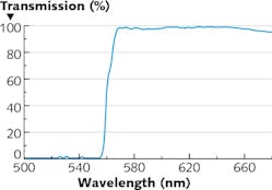
The function of a dichroic filter is to separate the spectral bands of both the excitation and emission light with minimal signal loss and minimal spectral gap between bands (see Fig. 4). Sharp transitions from reflection to transmission enhance image contrast for many applications, including fluorescence and multispectral bioimaging. For implementation in these systems, dichroic filters must possess low angle shift, low polarization splitting, and excellent flatness of both reflected and transmitted wavefront to eliminate any noticeable focal shift, which could be detrimental to any imaging system. In life sciences, this is critical for applications such as total internal reflection fluorescence (TIRF) and structured illumination microscopy.Coating stress
A coating can alter the way in which an optic reflects and transmits light and, in some cases, it can change the form of the optic itself. Thin film layers produce interference effects, which can be used to manipulate the transmission or reflection properties of light within an optical system, allowing one to essentially choose which wavelengths they want to use. The film itself can be quite thin (<5 μm) or very thick (>30 μm), depending on the desired spectral response. Deposition of a coating normally produces stress within the thin film that can change in the flatness of the optical substrate-generally, the thicker the coating, the more stress. The type of stress—tensile or compressive—depends on the type of coating process used as well as details of the coating conditions. Typically, the effect of stress-induced curvature is to add a roughly spherical component (that is, a hill or bowl shape) to the shape of the substrate.
The effect of this curvature on an optical beam or image is to some degree like that of a lens and thus may introduce unwanted distortion into the optical system. For example, if an array of wells containing fluorescent DNA molecules is being imaged onto a CCD detector, then the position of each element of that array needs to be accurately known on the detector. This requires precise control of the curvature of each optical component in the system. This curvature can be measured using an optical interferometer (see Fig. 6).A number of techniques can be used to offset stress-induced curvature. The simplest fix may simply be to increase the thickness of the substrate. The use of additional techniques adds cost; sometimes tolerating a repeatable stress, preferably low in level, is crucial to keep yields high and costs low.
The optical distortion introduced by the curvature of a coated element affects light transmitted and reflected by the element. In addition, any variation in thickness, parallelism, or index of refraction across the part will result in distortion. Most life science customers are concerned with distorted light transmitted through the element, called transmitted wavefront error (TWE), although it's not uncommon to specify reflected error, or flatness, for certain applications. Either can be measured using an interferometer (see Fig. 7). Traditionally only of interest when characterizing substrates, recent advances in instrumentation design have driven the levels of performance such that measureable amounts of TWE and flatness related to the coating itself need to be carefully managed.Cost and selection
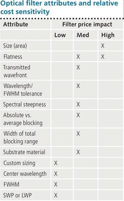
Many factors directly affect the cost of a filter, particularly in volume production. While most requirements are often common and straightforward, sometimes unanticipated costs and corresponding price impacts are incurred by using specifications that are intuitively not linked to a higher price. The table indicates relative sensitivity of some common filter attributes and their impact on pricing.In any case, it is helpful to understand the fundamentals so that you can select filters that will enable the best outcomes for your experiments, troubleshoot your current setup, and/or work with a provider to develop custom components. For all of these situations, there is plenty of expertise available to support your needs—just ask!
REFERENCE
1. Alluxa technical paper, "New metrology techniques for advanced thin film optical filters"; see http://bit.ly/1Ng2wrv.


