Materials that suffer from negative thermal effects during nanosecond laser machining can potentially be machined by picosecond lasers with a much higher quality.
JEFFREY SERCEL, JOHN BICKLEY, and JOSHUA STEARNS
When discussing materials processing, the term "ultrafast lasers" is often used to describe picosecond and femtosecond lasers in applications where the laser pulse length is shorter than the time taken for absorbed laser energy to diffuse into the substrate, or typically 5 to 10 ps. Ultrafast laser processing is growing in popularity because of the good cosmetic finish that can be obtained (due to lower heating and reduced debris-related damage), the enhanced coupling due to nonlinear intensity-dependent absorption, and the relative ease with which the machining result can be achieved.
There are many examples of high-quality parts that have been machined with ultrafast lasers (see Fig. 1). Compared with longer-pulse alternatives, however, picosecond lasers have low average power and a higher cost per watt, and they can be slower for machining when larger volumes of material are to be removed. There are rare cases, such as single-pulse ablation of thin films above semiconductor regions, where short-pulse lasers are uniquely able to remove material without causing heat damage to the underlying p-n junction. In other cases, a well optimized nanosecond laser process may deliver equivalent or acceptable quality, higher throughput, and far more cost-effective results.
Comparing an unoptimized nanosecond process to a highly optimized picosecond process, as seen in some ultrafast laser sales literature, can be misleading. This article discusses some of the complexities that need to be understood when implementing a production-worthy process.
Cold ablation
In explaining the term "cold laser ablation," it is frequently said that the high peak energy density in the short laser pulse results in an adiabatic process, with heat being removed through the ejection of ablated materials. With ultrafast lasers, nonlinear intensity-dependent multiphoton processes cause optical breakdown of otherwise transmissive or reflective surfaces to enable laser-energy absorption controlled methods. However, a small percentage of residual laser energy can generate heat. At high repetition rates or higher power densities, this heat buildup can lead to melting and charring, driving the need for high-speed scanning.
For materials with defined bandgaps such as semiconductors, photonic ablation occurs when atoms are excited into higher quantum states through the absorption of energy. When the energy of a single photon meets or exceeds the bandgap of the target material (quantum absorption energy), the laser energy can be absorbed, the exposed material is vaporized, and heat and debris are carried away in the plasma in a cold ablation process.
Cold ablation can be considered as a balanced heat equation. It can be achieved by optical absorption of laser energy at virtually any wavelength. The high conversion efficiency of single-photon absorption should not be overlooked when developing a robust micromachining process, which typically starts with determining the wavelength of laser to be used (see Fig. 2).
When the material bandgap exceeds the energy of a single photon, multiphoton absorption is required for cold ablation. Short pulse length with high photonic energy provides a statistical advantage in achieving multiphoton absorption, but as the number of photons required to reach the quantum absorption energy increases, the efficiency of energy combination will typically decrease.
When multiple photons arrive at a material simultaneously and with high electromagnetic-moment phase integrity, the result is more efficient multiphoton process coupling of their energies. However, differences in electromagnetic moment phase purity (similar in concept to spin de-phasing) reduce the effectiveness of the energy summation process. We call this effect the hyper-fine phase purity of the laser pulse, and it seems to vary in different lasers to different degrees. This parameter is not typically discussed and not quoted on data sheets. This level of coherence is not covered by the m2 parameter such that lasers having identical specifications from two manufacturers can be set to equivalent pulse characteristics yet have significantly different multiphoton coupling characteristics due to hyper-fine phase purity, which can be detected in materials such as crystalline sapphire.
For the user, it is critical to evaluate lasers in this regard through material interaction parameterization tests. In general practice, the fewer photons required to add up to a bandgap the better. For high-order multiphoton processes, lasers with a longer gain medium, or lasers operated in a more quiescent gain regime, seem to have better multiphoton coupling.
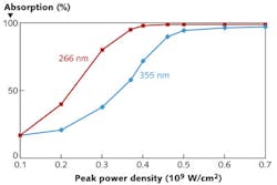
With a high enough peak laser power, material surface characteristics can be changed such that subsequent laser energy will be absorbed and machining will occur. For example, dynamic absorption of 355 nm photons can be compared to that of 266 nm photons in a high-bandgap (9.9 eV) optically transparent material (see Fig. 3). In this example, a power meter placed behind the sample records the transmitted laser energy at increasing levels of peak power density.
Normally, the sample is transparent to 355 nm pulses at 3.5 eV and 266 nm pulses at 4.6 eV photon energy—the former representing a three-photon process and the latter a two-photon process for the 9.9 eV bandgap. At low energy density, both wavelengths transmit at similar levels. As the energy is increased, the 266 nm two-photon process couples more efficiently, being at 50% absorption by 0.19 GW/cm2, compared to 355 nm reaching the same absorption level at 0.34 GW/cm2. By 0.5 GW/cm2, both wavelengths reach absorption saturation. Note that the 266 nm wavelength has higher absorption than the 355 nm wavelength in all cases.
One variable parameter for laser materials processing when optimizing a process is repetition rate. When operating at 100 kHz and a pulsewidth of 10 ps, a laser has a duty cycle of 1 in 106. It would seem obvious that to increase process speed one would simply increase the repetition rate; however, undesirable effects can occur at high repetition rates. One is the interaction of the laser pulse with the debris plume from the prior pulse, sometimes referred to as plasma shielding. This causes the material removal to become less effective and can also cause laser scattering and debris formation.
Another effect of higher repetition rate is (power density) heat accumulation. Multiphoton coupling is usually not 100% efficient. Even a small fraction of 1% pulse energy is converted to heat and remains in the material, a repetition rate of 100 kHz will result in material heating, and a multimegahertz laser will potentially eliminate any cold benefits of short-pulse laser processing. Operating at higher repetition rates with short pulses therefore will melt materials if confined to a small area by slow scanning.
Scanning requirements
The need to dissipate heat from high-repetition-rate lasers is the primary driver for scanning requirements. A 15 μm spot with 100 kHz repetition rate and 30% pulse overlap needs to move at slightly over 1 m/s. With galvanometer scanners offering speeds up to 5 m/s for a relatively long F-theta objective, performance is adequate for machined areas that are smaller than the deflection field (approximately 110 mm), and where positional accuracies on the order of ±20 μm are acceptable.
Clearly, higher repetition rates or reductions in field size to achieve better positional accuracy challenge this performance; this has prompted equipment engineers at IPG Microsystems to develop galvanometer-based scanning methodologies that overcome traditional limitations. As a general rule, however, galvanometer scanning for machining of relatively large flat areas provides the highest volumetric material-removal rates.
Satisfying the dual requirements of accuracy and speed is a major concern. When precisely machining small features, a better alternative to galvanometer scanning is a high-optical-resolution fixed-beam delivery system combined with a precision X-Y stage that moves the part under the stationary beam. This configuration provides the smallest-diameter beam and delivers the best positional accuracy. Here, the example 1 m/s requirement can be met by a mechanical stage, but issues of acceleration time and system vibration can become problematic.
One solution to the accuracy and speed challenge is to use a shaped beam. An optically created long, very narrow beam having virtually uniform energy density along its length has a machining effect similar to exposing many individual round beams in parallel. The machining-rate gains from this parallelism can enable lower repetition rates and lower part-movement speeds, thereby overcoming the plasma-shielding issue and reducing localized heating because the energy is distributed over a larger area. Additionally, a reduction in the width of the point-spread function, which effectively narrows beamwidth, and the replacement of the partially overlapping Gaussian pulses with a smooth-sided line beam gives greatly improved edge acuity.
Micromachining with a shaped beam allows optimal use of the energy density with the available laser power, adjusting the dose to provide carefully controlled minimal heat accumulation, while spreading the available energy over a large area to achieve the required throughput. Line-beam processing will frequently allow the use of a lower-priced laser than would otherwise be the case, in addition to reducing the cycle time per part.
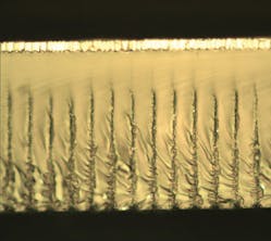
Finally, picosecond lasers can enable machining techniques that do not rely on ablation. In the scribing of sapphire wafers for singulation of LED devices, a picosecond laser can produce results with excellent sidewall profiles. However, cutting through wafers several hundred microns thick requires large numbers of pulses, and therefore time. In patent-pending (December 2009) technology known as QuieScribe, IPG Microsystems has taken advantage of the characteristics of ultrafast lasers to channel the energy into the crystal structure of the wafer, achieving deep single-pulse penetration and crystal cleaving of the material (see Fig. 4). QuieScribe methods provide a several-orders-of-magnitude gain in throughput over the conventional ablation separation processes.
When correctly optimized, picosecond processing can achieve results that are not available with other techniques. Successful implementation requires an understanding and characterization of material-photon interactions, time-dependent process-rate variations, and sample handling, if potential benefits are not to be compromised by conflicting system demands. Working with equipment vendors that perform parameterization studies using a range of laser types, both picosecond and longer pulsewidth, while taking a system-level approach to scanning architectures and equipment configuration, is highly recommended if implementing high quality, cost-effective micromachining is the long-term goal.
Jeffrey Sercel, John Bickley, and Joshua Stearns are with the Microsystems Division of IPG Photonics Corp., 220 Hackett Hill Rd., Manchester, NH 03102; e-mail: [email protected]; www.ipgphotonics.com/microsystems.


