JEFF HEBB
Thermal processing has always played a key role in the formation of complementary metal-oxide semiconductor (CMOS) transistors, especially for critical processes such as ultrashallow junction (USJ) activation and silicide formation. The scaling of devices to smaller dimensions has generally demanded the introduction of semiconductor thermal processing equipment that can deliver both thermal profiles with higher temperatures for higher dopant activation (faster transistors) and shorter processing times for less diffusion (smaller transistors).
Two main types of annealing equipment are used today to execute these critical anneals. The first is conventional rapid thermal processing (RTP), where a single wafer is heated by tungsten halogen lamps to temperatures between 300°C and 1050°C on time scales of 1 to 30 s. The RTP method has been part of mainstream semiconductor manufacturing for more than 20 years and has enabled USJ scaling starting at the 130 nm node. The second and most recent advance in thermal processing equipment is millisecond annealing, where the wafer is typically brought to temperatures between 1100°C and 1350°C (just below the melting point of silicon) on time scales of hundreds of microseconds to several milliseconds.
Annealing challenges
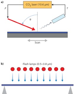
Millisecond annealing (MSA) is accomplished using two different approaches: laser spike annealing (LSA) or flash lamp annealing (FLA). In LSA, a long-wavelength carbon-dioxide (CO2) laser beam is incident to a semiconductor wafer at a grazing angle to form a “line beam” at the wafer plane that scans back and forth across the wafer (see Fig. 1). In FLA, the whole wafer is illuminated in a single instant by a bank of flash lamps—similar to RTP except on a much faster time scale. For both USJ and nickel silicide formation, each method has its own current and future challenges.For USJ formation, MSA was introduced into logic manufacturing about 5 years ago and is now mainstream in high-volume manufacturing for the 40 and 28 nm logic nodes. In the most basic scheme, an RTP spike anneal followed by MSA achieves diffusion and activation of the source/drain (SD) and source/drain extension (SDE).1 The RTP step diffuses the extension under the gate, which sets channel length and also anneals out any end-of-range (EOR) damage caused by ion implantation to reduce junction leakage. The MSA step—with very little diffusion—enhances activation of both SD and SDE. The junction depth (channel length) and dopant activation are essentially decoupled. As devices scale to smaller dimensions, spike RTP temperature is typically lowered to reduce dopant diffusion and manage short-channel effects. In addition to this one-step integration scheme, advanced multistep MSA integration schemes are used in production, with transistor drive-current gains greater than 10% reported.2
Temperature uniformity requirements for the RTP spike anneal and MSA steps are quite stringent because these steps define channel length and series resistance of the transistor. The within-wafer temperature uniformity and repeatability requirement for the RTP spike anneal is approximately 3°C (3σ). For MSA, the process window is wider because the process is diffusionless, but large variations in activation will degrade yield. These requirements can typically be met on monitor wafers, but on real device wafers, the situation is different.
One challenging issue that degrades temperature uniformity for both RTP and MSA is “pattern effects”—differences in optical absorption caused by the device patterns create within-die temperature nonuniformities, degrading performance and yield.3 Driven mainly by thin-film interference, pattern effects can be severe for large differences in reflectivities between the film stacks at short wavelengths. For RTP, effective solutions are achieved through equipment design—such as avoiding direct illumination of the patterned side of the wafer by heating the wafer from the backside where there are no patterns. For MSA, these solutions do not apply because the patterned side must be illuminated for the process to take place.
Lasers and flash lamps
Laser spike annealing minimizes pattern effects through its specially designed laser source and optics: The laser’s long wavelength (10.6 µm), p-polarization, and Brewster’s angle of incidence have all been shown to drastically reduce pattern effects. Flash lamp annealing uses a short-wavelength source (0.5–0.8 µm) and pattern effects are minimized using antireflection (AR) coatings or “dummification,” whereby dummy structures are patterned on the die for more uniform light absorption. Dummification is suitable for a manufacturing environment with a low product mix, as it requires changes to the mask set for each product. Without AR coatings or dummification, pattern effects can be >100°C for FLA, whereas pattern effects for LSA are approximately 10°C.4
As devices scale to smaller dimensions, IC manufacturers get more aggressive with various forms of strain engineering, such as embedded silicon germanium. One requirement of MSA is compatibility with advanced strain engineering: The introduction of any MSA step cannot negate the positive effects of the strain on mobility, or create any other negative side effects.
One side effect observed on wafers with aggressive strain engineering after MSA is lithographic overlay errors. Transient stress generated during the anneal causes dislocations to form and nucleate, causing plastic deformation and overlay errors during the next lithography step. Although reducing MSA peak temperature resolves this issue, device gain is lost. One manufacturing solution for LSA is to reduce annealing time by simply increasing stage speed.5 Another potential solution is “dual-beam LSA” where a second wider laser beam is introduced to decrease transient stress during temperature ramp.6 For FLA equipment, backside heating via RTP lamps can decrease transient stress during the ramp to peak temperature.
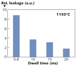
When USJs are scaled beyond 28 nm, the combined RTP spike anneal and MSA can cause too much diffusion and short-channel effects. However, a conventional MSA step alone is not long enough to effectively anneal out the EOR damage from ion implantation that can lead to junction leakage. So MSA suppliers are widening the process window of MSA tools to time regimes on the order of 10 ms—an order of magnitude greater than conventional MSA. Fortunately, dual-beam LSA achieves this goal. In the case of defect annealing, the second beam is much wider than the CO2 beam, enabling a dwell time on the order of 10 ms. Junction leakage is reduced by a factor of four compared to a conventional anneal at 0.8 ms (see Fig. 3). Flash lamp annealing tools also can anneal at longer dwell times by programming the lamps to fire with a longer time profile.7Nickel silicide formation is also presenting new thermal processing challenges in wafer manufacturing as devices scale to smaller dimensions. Conventional nickel silicide formation consists of two low-temperature RTP steps with a selective etch in between. As devices scale to 28 nm and beyond, nickel diffusion during the second RTP step can cause junction leakage and yield loss.8 A promising solution is to replace the second RTP step with MSA, which reduces nickel diffusion due to the short time scale.9 For this application, a second type of commercially available laser annealing tool uses a short-wavelength diode laser at near-normal incidence.
The nickel silicide application presents two new challenges for MSA: low-temperature process control (600°C to 900°C) and pattern effects in the presence of a metal silicide. Regarding process control, the LSA tool architecture incorporates closed-loop real-time wafer temperature control; modifications made to the measurement and control system accommodate the change in temperature range.10 Alternatively, the FLA and diode laser annealing (DLA) system run in open-loop power mode and carry a higher production risk. Regarding pattern effects, it turns out that the conclusions are essentially the same as for USJs. The LSA tool architecture effectively minimizes pattern effects due to the laser and optics design, whereas FLA and DLA will have large pattern effects due to their short-wavelength sources unless antireflection coatings or dummification are used.
Millisecond anneal and RTP will play a critical role in meeting requirements for development and manufacturing of logic ICs at the 20 nm node and beyond, as they do today at 28 nm. Device shrinkage and changes in architecture are bound to create unforeseen challenges and new opportunities for advanced annealing. MSA suppliers can best meet these challenges by expanding the application space of their equipment and focusing on stringent demands on process control.
REFERENCES
1. S.K.H. Fung et al., Symp. VLSI Technol. Dig., 92 (2004).
2. T. Yamamoto et al., IEDM Technol. Dig., 143 (2007).
3. L.M. Feng et al., Proc. Int. Workshop Junct. Technol., 25–30 (2006).
4. T. Miyashita et al., IEDM Technol. Dig., 1–4 (2009).
5. S. Shetty et al., Proc. Int. Workshop Junct. Technol., 119 (2009).
6. Y. Wang et al., Proc. Int. Workshop Junct. Technol., 18–24 (2010).
7. H. Kiyama, Proc. Int. Workshop Junct. Technol., 25–31 (2010).
8. C. Ortolland et al., IEDM Technol. Dig., 23–26 (2009).
9. Y.W. Chen et al., Proc. IEEE Int. Conf. on Adv. Thermal Processing of Semicon., 213–216 (2009).
10. J. Hebb et al., to be published in Proc. IEEE Adv. Semicon. Mfg. Conf. (2011).
Jeff Hebb is vice president of laser product marketing at Ultratech, 3050 Zanker Rd., San Jose, CA 95134; e-mail: [email protected]; www.ultratech.com.


