For decades, smaller has meant better in semiconductor electronics. Moore’s Law says that the number of transistors on a chip should double every two years, which requires shrinking component geometry by 30% at the same time. For developers seeking to sustain that trend for a few more generations, extreme-ultraviolet (EUV) lithography has become the “holy grail.”
In the fabrication of chips, photolithography involves projecting the image of an original mask onto a light-sensitive material called photoresist, then chemically etching the resulting pattern into a semiconductor substrate. Optical lithography started with visible light sources, then shifted to ultraviolet mercury lamps, 248 nm krypton-fluoride lasers, and finally—around 2001—to the 193 nm argon-fluoride laser, which initially wrote features with a nominal size of 130 nm. (Feature measurements have changed since then; see “Semiconductor technology steps,” below).
The next technological step was supposed to be the 157 nm molecular-fluorine laser, but problems with the calcium fluoride optics required at that wavelength proved daunting. Instead, developers turned to tricks such as immersion lithography, which achieves a sharper focus of the 193 nm line by directing the light through water. Refinements to immersion lithography allowed fabrication of circuits with a 45 nm half-pitch, and adding a trick called double-patterning can shrink the half-pitch to 32 nm in the new generation of fabrication lines coming on line this year. The next step down in size was supposed to require sources emitting at 13.5 nm in the EUV, but last year Intel (Santa Clara, CA) decided instead to refine 193 nm lithography one more time.
It’s another in a long series of slips for EUV lithography. A handful of EUV systems are running in labs, but the technology isn’t ready for production, with power levels and mask defects among the key issues still to be resolved. However, developers remain optimistic that the issues are matters of engineering rather than fundamental problems.
EUV sources
The roots of EUV lithography go back more than 25 years, says Stefan Wurm, associate director of lithography at the Sematech Research Test Center (Albany, NY), an industry research consortium. Developers settled on the 13.5 nm source wavelength about a decade ago because that was the part of the EUV where the best optics were available. Solids and gases strongly absorb EUV, and the best mirrors are silicon/molybdenum (Si/Mo) multilayers with peak reflectivity at 13.5 nm.
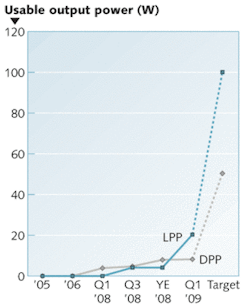
Complex laboratory lasers and high-harmonic sources can generate EUV, but tin plasmas produce much more power at 13.5 nm, and are better suited for production. “Industry has been going back and forth between laser-produced and discharge-produced plasmas,” Wurm says. The first experimental lithography tools used laser sources, but the second-generation prototype tools such as the one Sematech uses in Albany are excited by discharges. Now laser-produced plasmas have moved back into the lead because they appear easier to scale to higher powers (see Fig. 1). Excimer and Nd:YAG lasers have been tested, but Wurm says CO2 lasers have become the leading choice because they convert more pump power to EUV and generate the right pulse structures.
The test systems can generate up to 20 W of EUV power for days, enough for research and producing test chips. Commercial systems need throughput of about 100 wafers/hour around the clock, so they would require about 180 W of EUV power sustained for a year, says Bryan Rice, director of lithography at Sematech. Attaining that level will require an 8 kHz pulsed CO2 laser emitting average power of 10 to 20 kW.
High mirror losses drive the power requirement. Projection optics with 40 to 50 pairs of Si/Mo layers can achieve reflection of close to 70% at normal incidence, close to the theoretical limit of 71% to 72%. But the losses are much higher because the complex projection systems include many such mirrors. Five to six mirrors are needed to focus the EUV onto the mask, and a further six mirrors are needed to project the mask onto the chip, so only a small percentage of the EUV from the source actually reaches the chip.
Performance, defects, and design
Extreme-UV sources and optics are not the only challenges. Such short wavelengths mean tighter tolerances, more sensitivity to defects, and new design challenges.
“Once the sources are in place, the real issue will be mask quality,” says Wurm. Lithography replicates a mask many times on a wafer, so every mask defect is replicated many times. A single “killer” defect in one of the four chip patterns on a mask means that one-quarter of the chips produced are defective, so specifications for masks are very, very tight, says Rice.The smaller the geometry, the fewer atoms need be out of place to cause a killer defect. Even worse, the thin pellicles that protect masks from dust particles in current 193 nm system are not usable at EUV wavelengths. That means EUV systems will need much tighter particle control than previous generations.
Extreme-UV also will require a new generation of inspection systems to spot defects in substrates, blanks, and finished masks, as well as repair tools. At the European Mask and Lithography Conference (Dresden, Germany) in January, Wurm put inspection among major industry concerns about the readiness of EUV for pilot production lines in 2010 to 2012.1 However, he reported “impressive progress over the past two years” in chemically amplified EUV resists, including resolution below 22 nm. Sematech’s timetable for introduction of new technology into production shows pilot production of 32 nm chips is expected to begin this year (see Fig. 2).
Nor is hardware the whole story. Each new generation of lithographic systems requires a new generation of chip-design software to make silicon into circuits. Software has become increasingly critical to the production of high-performance chips as feature geometry shrinks and chip complexity increases, says Milind Weling, engineering director of Cadence Design Systems (San Jose, CA), a major electronic-design-automation software house. The software gives designers “a whole platter of tricks” to shape on-chip structures to behave as desired, he says. The software crunches tens of gigabits of data to design chips and needs updating to incorporate fresh tricks for each generation of chip geometry.
Challenges
Extreme-UV has been a long time coming, and 193 nm systems have been stretched far beyond their expected limits. Back in 1997, Solid-State Technology predicted that EUV would be needed to fabricate chips with 65 nm geometry, Weling notes. Now EUV is thought necessary when half-pitch reaches 22 or 16 nm. “Every year it seems like six years from now it will be ready,” he adds.
Some industry observers are growing cynical. Intel’s decision last year to skip EUV for the generation it plans to introduce about 2011 and discussion during EUV lithography panels at the SPIE Advanced Lithography meeting in February both sparked negative news stories. Yet it’s also clear that conventional lithography has been stretched to its limits. Extreme-UV looks like the best hope to push Moore’s Law further.
“I am extremely encouraged by what EUV has to offer,” says Weling, citing the big improvement in resolution from moving to 13.5 nm. Wurm hopes that EUV pilot-production of next-generation chips, with half-pitch of 22 nm, can be demonstrated by 2011 or 2012, with production to start in 2013 or 2014.
Even at Intel there’s hope. “If I thought EUV problems were unsolvable, I’d be looking for another job,” says Michael Mayberry, Intel’s vice president of technology and manufacturing and director of components research. “We have confidence we can make 193 nm extend another generation,” by using multiple patterning. But he believes EUV will be the next step. “We’re in the engineering space, as opposed to requiring new inventions space,” he says. “I believe EUV will be available for production early in the next decade.”
Extreme UV won’t have the field to itself. Efforts continue to push conventional lithography to smaller fractions of the wavelength. In April, Rajesh Menon’s group at the Massachusetts Institute of Technology (Cambridge, MA) demonstrated a new way to write lines only about 1/10th of a wavelength wide in photoresist with an ultraviolet laser.2 Yet if past history is any guide, these new ideas will take years to reach the production stage. With huge sums already invested in EUV, and the semiconductor industry dependent on further reductions in chip feature size, it may be EUV or bust.
REFERENCES
- S. Wurm, “Lithography Development and Research Challenges for the =/< 22 nm half-pitch,” paper presented at European Mask and Lithography Conference held in Dresden, Germany (Jan 2009)
- T. L. Andrew et al., Science Express, April 9, 2009; doi: 10.1126/science.1167704
- F. M. Schellenberg; Bruno M. La Fontaine editors, 2009 Proc. of SPIE 7271 (2009)
Semiconductor technology steps
Each generation of semiconductor technology traditionally has been identified by the minimum feature size on chips, with the target values dropping about 30% each step thus doubling the number of transistors per unit area. In recent years, however, actual feature sizes have diverged from the oft-cited “nodes,” leading the International Technology Roadmap for Semiconductors (www.itrs.net) to drop that term in 2005. Lithography specialists now measure minimum chip feature size as “half-pitch,” one-half of the center-to-center distance between parallel conductors on a chip, which in practice is larger than the nominal node size. For example, a system built for the 22 nm node may fabricate chips with 32 nm half-pitch.
Chip manufacturers largely have retained the old “node” designations because they consider feature sizes proprietary, and don’t disclose half-pitch. A further complication is that feature sizes differ among types of integrated circuits fabricated with the same generation of lithographic systems. Features on nonvolatile flash memories, for instance, are smaller than those for dynamic random-access memory (DRAM), and both are smaller than those on microprocessors.
In an effort to be consistent, this article specifies half-pitches for current and future generations of lithographic systems.

![FIGURE 2. Sematech’s timetable for high-volume manufacture of future chip generations (measured in half-pitch) shows production of 45 nm chips has already begun, but only on a small scale; pilot production of 32 nm chips is expected to begin this year. ML2 is maskless lithography, one of several emerging technologies [1]. For more on emerging technologies, see the SPIE Advanced Lithography proceedings [3]. FIGURE 2. Sematech’s timetable for high-volume manufacture of future chip generations (measured in half-pitch) shows production of 45 nm chips has already begun, but only on a small scale; pilot production of 32 nm chips is expected to begin this year. ML2 is maskless lithography, one of several emerging technologies [1]. For more on emerging technologies, see the SPIE Advanced Lithography proceedings [3].](https://img.laserfocusworld.com/files/base/ebm/lfw/image/2016/01/th_320268.png?auto=format,compress&fit=max&q=45&h=144&height=144&w=250&width=250)
