Detectors having performance similar to those made on rigid silicon substrates have been successfully fabricated, packaged, and tested.
The future will provide many applications for sensors and associated electronic circuitry on flexible substrates. Potential applications include "smart fabrics"—fabrics with embedded sensors for future attire—and ready-to-use sensor arrays that could be placed onto nonplanar surfaces of robots for increased perception. Sensors on flexible arrays might serve as inexpensive upgrades by readily adapting to existing surfaces without the need for major structural alterations. Thanks to miniaturization, much more can be packed into much smaller areas, providing richer information, greater redundancy, and reliability at lower cost.
The Microsensors Lab at the University of Texas at Arlington is developing "smart skin"—a flexible substrate that incorporates electronic sensors for measuring temperature, flow, acceleration, pressure, and the associated electronic circuitry. Microbolometers are incorporated on flexible substrates to make the smart skin sensitive to temperature and broadband IR radiation.
The flexible substrate we used is a polyimide, which has excellent resistance to most silicon process chemicals, is thermally stable relative to the potential applications, and is a tried and tested substrate in the electronics industry. We initially used solid polyimide sheets as the substrate but we are now using liquid polyimide to spin-cast the substrates. Detectors with performance similar to those made on rigid silicon substrates have been successfully fabricated, packaged, and tested.
Thermal detectors
All objects radiate energy, which can be detected by suitable optical detectors; the magnitude varies in different parts of the electromagnetic spectrum and is a function of the object temperature. In a bolometer, the incident IR energy causes the temperature of the detector to change, altering the detector's electrical resistance. Metals, semiconductors, or superconductors can be used as detector materials.
We have used semiconducting yttrium barium copper oxide (YBCO) as the detector material. A simple bolometer consists of a temperature-sensitive element or thermometer (YBCO in this case) with a fixed DC bias across it. The resistance of the bolometer is measured as the modulating signal of the bias. The change in the bolometer resistance, ΔR, depends on the heating of the thermometer by the incident radiation. Hence, reducing heat losses from the detector element improves the performance/sensitivity of the detector. Thermal isolation of the detector from the ambient is thus a critical design requirement. This is accomplished by suspending the thermometer above the substrate by micromachining. Microbolometers can achieve high responsivities at room temperature as a result of micromachining the thermal-isolation structure and vacuum packaging to reduce their heat loss.
Fabrication
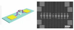
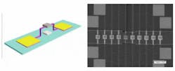
The fabrication of microbolometers on flexible substrates begins by spin-casting the flexible substrate on a silicon-wafer carrier with liquid polyimide. This process allows conventional silicon microfabrication equipment to be used to fabricate the sensors on flexible substrates. In our case, the polyimide substrate is spin-cast to be 40 µm thick—about the thickness of a human hair. The polyimide substrate is passivated and the microbolometer is fabricated using surface micromachining with a polyimide sacrificial layer (see Fig. 1).
After removing the sacrificial polyimide, the microbolometer is suspended above the substrate and supported by titanium (Ti) electrode arms. The Ti arms connect the detector to large gold (Au) bond pads. For an electric conductor, titanium has low thermal conductivity. A mirror underneath the suspended thermometer forms an optically resonant cavity to increase the optical absorption of the sensor. The height of the resonant cavity is determined by the thickness of the sacrificial polyimide, which can be adjusted during the fabrication process.
Generally, bolometers are wideband detectors. Depending on the application, their performance can be optimized at different IR wavelengths. This is accomplished using the same metal mirror under the detector, which acts as a reflector for incident IR energy. The resonant wavelength of the detector depends upon the mirror-detector separation.
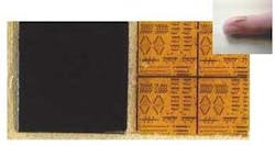
Upon completion of the microbolometer fabrication process, the polyimide substrate is removed from the silicon-wafer carrier, yielding sensors on a substrate (see Fig. 2). Substrates have been bent to a 1.5-mm radius of curvature without any apparent change in the microbolometer characteristics.
Figures of merit
The temperature coefficient of resistance (TCR) is the normalized change in resistance per unit change in temperature. The YBCO thermometers have exhibited a TCR of approximately -3% K-1 at room temperature. The responsivity falls off at higher frequencies because of the thermal time constant of the microbolometer, generally in the range of milliseconds. Responsivity and detectivity as high as 5 × 10⁵ V/W and 108 cm-Hz1/2/W, respectively, have been measured with 1-µA bias in the microbolometers on flexible substrates. The thermal conductance G of the microbolometers was measured to be as low as 0.4 µW/K, a measure of the thermal isolation. These values are comparable to those of similar microbolometers fabricated on rigid silicon substrates.
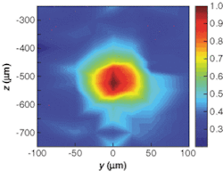
To demonstrate the capabilities of the microbolometers on a flexible substrate, a microbolometer was scanned over the image of a point source. This technique was used because the microbolometers have not yet been integrated with any readout electronics on the flexible substrate and it demonstrates the ability to gather a simple image (see Fig. 3). The point source was achieved by placing a pinhole in front of a broadband mock blackbody IR source and using a convex lens to focus the point source onto the microbolometer image plane. The sensor output is in an area comparable to its size.
Future plans
The next step in the development of microbolometers on flexible substrates would be fabrication of microbolometers that can be encapsulated in a vacuum cavity at the device level. This will result in wafer-level packaging for the microbolometer arrays. The sensors perform best when the heat loss from the sensor is minimized by micromachining a thermal-isolation structure. While physically isolating the sensors from the substrate contributes toward this end, the microbolometer performance reaches its full potential only when the devices are operated in a vacuum.
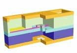
The detectors currently are placed in bulky and expensive vacuum packages for optimum performance, which defeats the main purpose of sensors on a flexible substrate. Work is under way to design a microbolometer in a vacuum—hermetically sealed in a polyimide package at the device level (see Fig. 4). Challenges include the integrity of the circuit on the flexible substrate and the hermetic seal containing the vacuum bubble.
Encapsulating the microbolometer in a vacuum bubble and having a polyimide superstrate will increase the detector performance electrically and provide more mechanical strength to the crucial circuit in the detector plane. With suitable materials and thicknesses, the detector can be placed in a no-strain plane. Another issue for study is the optical transmission characteristics of the superstrate. Tests on polyimides have found that different polyimides have different transmission windows. The encapsulated detectors will have to be designed so that they operate in one of the superstrate optical pass bands.
In the future, microbolometers on flexible substrates can be integrated with thin-film-transistor technology to produce intricate microsystems that could provide interesting possibilities.
ACKNOWLEDGMENT:
The authors would like to acknowledge the contributions of Shadi Dayeh to the development of microbolometers on flexible substrates while he was at UTA. This work is based in part upon the work supported by the NSF under grant ECS-0245612.
AAMER MAHMOOD is a graduate research assistant and DONALD P. BUTLER and ZEYNEP CELIK-BUTLER are professors in the Electrical Engineering Dept. at the University of Texas at Arlington, Electrical Engineering Dept., Arlington, TX 76019; e-mail: [email protected].
