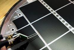
Researchers at the Fraunhofer Institute for Solar Energy Systems (Fraunhofer ISE; Freiburg, Germany) together with EV Group (EVG; St. Florian am Inn, Austria) have successfully manufactured a silicon-based multi-junction solar cell with two contacts and an efficiency exceeding the theoretical limit of silicon solar cells.
For this achievement, the researchers used a "direct wafer bonding" process to transfer a few micrometers of III-V semiconductor material to silicon (Si), a well-known process in the microelectronics industry. After plasma activation, the subcell surfaces are bonded together in vacuum by applying pressure. The atoms on the surface of the III-V subcell form bonds with the silicon atoms, creating a monolithic device.
RELATED ARTICLE: Emcore deploys 100th solar powered satellite
The efficiency achieved by the researchers presents a first-time result for this type of fully integrated silicon-based multi-junction solar cell. The complexity of its inner structure is not evident from its outer appearance: the cell has a simple front and rear contact just as a conventional silicon solar cell and therefore can be integrated into photovoltaic modules in the same manner.
"We are working on methods to surpass the theoretical limits of silicon solar cells," says Frank Dimroth, department head at Fraunhofer ISE. "It is our long-standing experience with silicon and III-V technologies that has enabled us to reach this milestone today." A conversion efficiency of 30.2% for the III-V/Si multi-junction solar cell of 4 cm² was measured at Fraunhofer ISE's calibration laboratory. In comparison, the highest efficiency measured to date for a pure silicon solar cell is 26.3%, and the theoretical efficiency limit is 29.4%.
The III-V/Si multi-junction solar cell consists of a sequence of subcells stacked on top of each other. So-called "tunnel diodes" internally connect the three subcells made of gallium-indium-phosphide (GaInP), gallium-arsenide (GaAs), and Si, which span the absorption range of the sun's spectrum. The GaInP top cell absorbs radiation between 300 and 670 nm. The middle GaAs subcell absorbs radiation between 500 and 890 nm and the bottom Si subcell between 650 and 1180 nm, respectively.
"Key to the success was to find a manufacturing process for silicon solar cells that produces a smooth and highly doped surface which is suitable for wafer bonding as well as accounts for the different needs of silicon and the applied III-V semiconductors," explains Jan Benick, team leader at Fraunhofer ISE. "The III-V / Si multi-junction solar cell is an impressive demonstration of the possibilities of our ComBond [trademarked] cluster for resistance-free bonding of different semiconductors without the use of adhesives," says Markus Wimplinger, corporate technology development and IP director of EV Group.
On the way to the industrial manufacturing of III-V/Si multi-junction solar cells, the costs of the III-V epitaxy and the connecting technology with silicon must be reduced. There are still great challenges to overcome in this area, which the Fraunhofer ISE researchers intend to solve through future investigations. Fraunhofer ISE's new Center for High Efficiency Solar Cells, presently being constructed in Freiburg, will provide them with the perfect setting for developing next-generation III-V and silicon solar cell technologies.
SOURCE: Fraunhofer ISE; https://www.ise.fraunhofer.de/en/press-and-media/press-releases/press-releases-2016/30-2-percent-efficiency-new-record-for-silicon-based-multi-junction-solar-cell

