FRANZ SCHUSTER, WOJCIECH KNAP, and VALÉRIE NGUYEN
The electromagnetic spectrum has historically been exploited using one of two kinds of technologies: optics for shorter wavelengths, and radio-frequency and electronics for longer ones. The terahertz region, which is situated between the optical and the electronic domains, has until recently remained mostly inaccessible due to the lack of practical sources and detectors (see Fig. 1).
Today’s strong interest in the terahertz region is motivated by the specific characteristics of terahertz radiation. The energy of a terahertz photon ranges around 4 meV, a value corresponding to vibrations of some heavy complex molecules, including explosives. Such low photon energies make terahertz radiation nonionizing; it is therefore considered to be safe in terms of health concerns.
Sensing techniques for the lower terahertz frequencies exploit the transparency of air and thin objects together with the high absorption coefficient of water. Imaging of items with high water content, such as people, animals, or plants, produces high contrast even through dry structures like clothes or paper. So it is possible to detect metallic (reflective) objects concealed under clothes. Many of these developments are strongly related to security concerns today, but a large future market is also emerging in industrial quality and food control.
Limitations of terahertz imaging
To capture an image, an optical system must generate an image of a scene, and a matrix of detectors sensitive to the desired wavelength placed at the location of this image will then measure the level of electromagnetic signal at each point of the image. In a camera or focal-plane array, the pixels should be spaced so they work independently, meaning that a pixel should not see details registered by the adjacent pixels. For the pixels to be independent, they should be spaced by a distance, determined by diffraction laws, of approximately 0.61 × λ × NA (the Airy disk radius), where λ is the wavelength and NA is the numerical aperture. In the case of visible light, this smallest possible pitch will range around 0.33 µm for an NA of 1. In the case of terahertz images the wavelength is much longer, and for a 1 THz image, the minimum pixel size becomes 183 µm. Only about 6 × 6 pixels can be placed in a square millimeter, leading to large focal-plane arrays if detailed images are necessary.
The CMOS pixel
To obtain an electrical-detection signal from a free-space terahertz wave, several approaches have proved to be adequate, technically speaking. These include the bolometer and the metal-oxide-semiconductor (MOS) transistor, each of which uses a completely different method of transforming the high-frequency wave into an electrical low-frequency signal.In a bolometer, the terahertz wave heats a temperature-sensitive detector such as a thermistor. The variation of resistance is measured, giving the variation of the terahertz energy flow on this pixel. The thermistor must be suspended in vacuum to retain the tiny amount of energy it receives for as long as possible (thermal insulation). Its construction is a specific and rather delicate process, leading to a very sensitive but expensive imager that can be adapted to almost the entire terahertz range.
The MOS-transistor-based pixel follows a completely different approach. No existing MOS transistor is able to respond at a frequency as high as 1 THz. However, even low-cutoff-frequency MOS transistors can rectify terahertz radiation, thanks to nonlinear properties of the charges/electron plasma in the transistor channel. Terahertz radiation perturbs the charge density and can lead to the creation of plasma waves as well as overdamped plasma oscillations. As a result, a continuous voltage appears between source and drain. In the simplest case (low carrier mobility and density), the process can also be understood in an electronic manner as a special type of resistive self-mixing.1
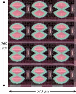
An antenna structure is needed to effectively couple the free-space terahertz wave to the subwavelength transistor. The whole structure can be realized with a standard complementary metal-oxide-semiconductor (CMOS) process, including the metal antenna, which is implemented in the metal interconnection layers (see Fig. 2). This ability to be processed with a standard industrial silicon technology is one of the main benefits of this approach.
Figure of merit
The sensitivity of the terahertz CMOS pixel determines the maximum image frequency and/or the minimum light of the terahertz source still detectable. It can be expressed using various terms, such as the noise-equivalent power (NEP) or the power sensitivity. The NEP represents the minimum detectable power for a given detection/noise bandwidth, and is defined by the incident radiation power leading to a signal-to-noise ratio (SNR) of 1 at the output of the detector. It is usually given in W Hz-1/2 to enable comparability between detectors with different noise bandwidths. The power sensitivity or responsivity, which is expressed in V/W, characterizes the ability of the pixel to convert the power received by the antenna into readable volts.
The best results obtained today with terahertz CMOS pixels at room temperature are a NEP of 8 × 10-12 W Hz-1/2 and a responsivity of 5 kV/W at 0.3 THz.2 To obtain this performance, each part of the signal chain must be carefully designed: the metallic antennas whose parasitic resistance becomes high at this frequency; the silicon substrate thickness, to control the reflection of the terahertz wave on the back of the imager; and the MOS transistor dimensions, which govern the impedance-matching with the antenna. Good results are found with not-so-small channel lengths—130 nm in this example. Losses increase with the frequency, and the highest measured operation today is slightly above 1 THz, with a sensitivity of 50 V/W for the same pixel.Applications
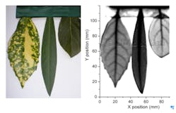
Mounted in a test package and used with a terahertz source for active illumination, the CMOS pixels provide images that emphasize the unique characteristics of terahertz radiation. Concealed objects in paper envelopes or in food products can be seen without the use of ionizing x-rays. Water-content sensitivity reveals the inner structure of a tree leaf, giving information on its health and water needs (see Fig. 3). Heterodyne detection in the terahertz domain and radar-like techniques can be applied to terahertz pixels to support 3D imaging.
Providing adequate terahertz illumination is still a major obstacle when very high powers are necessary, but compact solid-state sources already exist that allow easy illumination of small scenes at frequencies below 1 THz, opening the way to many applications in quality control and security. Small and standalone terahertz imagers, with the ability to be rapidly and reliably controlled directly at the place of interest, are now becoming a reality.
ACKNOWLEDGMENTS
The work described in this paper was carried out in collaboration with CEA-Leti, Grenoble, and the Laboratoire Charles Coulomb Common Research Unity of CNRS and Montpellier University. The authors acknowledge important contributions of B. Giffard and J.P. Rostaing from Grenoble and D. Coquillat and M. Sakowicz from Montpellier. The authors also acknowledge long-term support of this project from STMicroelectronics (Crolles, France).
REFERENCES
1. W. Knap et al., J. Infrared, Millimeter and Terahertz Waves, 30, 1319 (2009).
2. F. Schuster et al., Opt. Exp., 19, 8, 7827 (2011).
3. F. Schuster et al., “A Broadband Terahertz Imager in a Low-cost CMOS Technology,” Int. Solid-State Circuits Conf. (2011).
Franz Schuster is a PhD student at CEA-Leti (Grenoble, France) and at Montpellier University (Montpellier, France); e-mail: [email protected]. Wojciech Knap is research director at the Charles Coulomb Laboratory of the CNRS and Montpellier University (Montpellier, France); e-mail: [email protected]. Valérie Nguyen is program manager at CEA-Leti; e-mail: [email protected].


