ERIK NOVAK, STEPHEN HOPKINS, and ANDREW MASTERS
The solar energy industry is experiencing growth due to many factors, including high oil prices, government energy initiatives, and increasing worldwide desire to reduce greenhouse gas emissions and carbon footprints. World energy consumption is expected to double by 2050, and production of photovoltaic (PV) solar cells is rising at more than 40% annually. As with any industry, the key driver for commercial success is the overall cost to the end user, be it residential installations or grid-connected, utility-scale systems. For solar-cell manufacturers, this key driver is the cost per kilowatt-hour for electricity over the life of the system.
Multiple PV technologies are currently competing for share in the growing solar market. Traditional solar cells are made from crystalline silicon and remain the bulk of worldwide production. However, amorphous thin-film silicon, which can produce lighter, more configurable, but generally less efficient cells, is gaining share for production of solar cells. Couple that with additional PV technologies, including cadmium telluride (CdTe or "Cad-Tell"), copper indium germanium selenide (CuInGa(Se)2; also known as CIGS), and the highest efficiency (III/V triple junction cells), and it becomes clear that there are several viable technologies vying for a share of the solar energy market. And while each has its advantages and disadvantages, all share the need for precision surface metrology for quality control. Optical profilers are currently utilized by many PV manufacturers to increase yield and lower the overall production cost of solar cells through quantification, qualification, or monitoring of various process steps.
Texture characterization
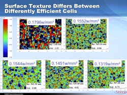
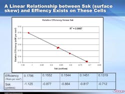
Texture is one of the critical surface parameters affecting solar-cell efficiency. A polished wafer of monocrystalline silicon (as in a bare semiconductor-grade silicon wafer) is about 40% reflective—depending on the wavelength of the incident radiation. A widely accepted technique to reduce this reflectivity is to texture (roughen) the surface so that reflected photons have a chance of being incident on another facet of the PV cell, creating another opportunity for PV interaction in the emitter layer. If the surface roughness is too great, however, then the mean free path (MFP) of the electron/hole pair may elongate to the point where the probability of them recombining reduces the overall efficiency.Trace and linewidth measurements
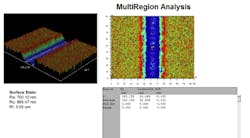
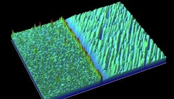
In addition to excellent vertical resolution and fast measurement times, noncontact optical profilers can segment data for evaluating critical properties on different levels of a sample surface. For solar applications, this is commonly used for trace and linewidth measurements. The quality and quantity of silver or other conductive traces used in solar cell production demands careful control to ensure proper performance of the panels, while minimizing the area obscured by nonphotovoltaic material. Furthermore, thicker or wider conductive traces actually increase the cost of manufacturing—due to the relatively high cost of silver paste—while decreasing the efficiency of the PV-cell. In addition, scribe lines, particularly in thin-film processes, are later filled with expensive conductive inks that then create the desired output power and current by "wiring" the various active areas. If the scribe lines are too shallow or deep, the wrong width, or in the wrong places, the panel's performance can be adversely affected. Identifying such defects prior to ink deposition allows material to be scrapped before too much value has been added.
Profiling software such as Veeco's Vision can be configured to automatically calculate line width, line spacing, depth, volume, and roughness within the trace and on the substrate, as well as log all parameters to a database with pass/fail capability for production control (see Fig. 2). These analyses can be performed on surfaces with one to several hundred critical features within the measurement.Optimization and control
Interferometric optical systems have a long history of use for quality control and process development/improvement for the process equipment used in solar manufacturing. Etch and deposition rates can be rapidly calculated across the wafer using the advanced automation capabilities of either the optical or stylus profilers. Heights of features are quickly measured at various locations across the substrate. This data provides feedback for both process control and optimization. A typical metrology application is the measurement of variations in height of stepped features across 8 in. wafers during deposition process development. Measurements can be taken and analyzed automatically across all positions. The data is then used to improve uniformity and the average height of critical features.
Veeco optical profilers also incorporate features that make them ideally suited for quantitative defect detection and analysis. Volume and/or height thresholds may be set by the user, and the software will automatically identify defects and can report on such features as height, diameter, volume, and X and Y maximum extent. By quantifying the surface defects, system users can determine where in the process they originate and work to optimize the process setup to eliminate them.
Film thickness
The thickness of varying substrate layers, both transparent and opaque, needs proper characterization, particularly for CIGS devices. The contact method utilized by stylus profilers provides very rapid and accurate film thickness measurements where there is a boundary, readily identifying the film-to-substrate distance. With their very low contact forces, Veeco Dektak profilers are able to do this without damage, even on soft polymers. More important, because it is a contact technique, the stylus profiler is insensitive to the material property differences that can create offsets in optical techniques if the materials are too thin or have differing absorption. This information is obtainable in only a few seconds, so it becomes practical to perform frequent checks on the process quality.
Due to their respective capabilities, stylus and optical profilers are often used in tandem for film thickness control. For example, the NT9100S optical profiler complements Dektak stylus measurements for film characterization in several key ways. Transparent film greater than about 2 µm in thickness can be measured across the entire sample surface. The optical system delivers faster area-based measurements, but if height offsets from the optical properties are present, the Dektak can be used to quickly calibrate the film. Then analysis software can automatically apply the offsets to future optical measurements. Additionally, the NT profilers can provide information on the surface roughness and defects for both the top and bottom surfaces of the films separately, so that the conformal properties of the film can be analyzed. Thus, the two systems work well together to ensure both film thickness and surface qualities are adequately characterized to improve and maintain peak performance.
Meeting the rapid advances in PV technology
The various technologies used for solar-cell manufacturing are advancing rapidly as researchers and corporations work to improve efficiency and drive costs lower. Accurate surface metrology of key features is a critical part of this process by enabling rapid surface and thickness metrology to subnanometer resolution to provide the data necessary to improve solar-cell development and production. Texture, step heights, trace widths, scribe widths, film thickness, and defect detection all assist manufacturing lines. Meanwhile, researchers can study material effects, environmental attack and fatigue, as well as perform sophisticated characterization to better understand the effect individual changes in the process equipment can have on the end products.
ERIK NOVAK is director of research of optical and industrial metrology, STEPHEN HOPKINS is a marketing communications specialist, and ANDREW MASTERS is VP, strategic marketing and business development at the Metrology & Instrumentation Group, Veeco Instruments; e-mail: [email protected]; www.veeco.com.


