BOB GRIETENS AND JISK HOLLEMAN
Light-emitting semiconductor structures have been used for a long time in the form of LEDs and, as efficiency has increased, they have made substantial inroads into illumination technology, competing with traditional lighting systems and enabling innovative illumination concepts. Despite their obvious maturity, however, they still have tremendous potential for further development.
At Twente University, the faculty for electrical engineering and the MESA+ Institute for Nanotechnology have jointly investigated the impact of electrical fields on lateral LED structures (see Fig. 1). In this structure, a gate electrode of polysilicon has been placed above the active light-emitting region. Operating the diode with constant current and a negative gate bias will cause it to shine more brightly. In addition, the intensity profile of the radiating surface is significantly altered. Thus, the light emission of an LED can be specifically varied via a MOS gate, which enables novel applications in illumination, measurement, and automation.
To understand the basic mechanism of this process, the structure must be modeled and compared with the experimental results. The more precise and meaningful the results of this comparison are, the more accurate the modeling will be. Often the indication of mere intensity data across the various surface elements is not sufficient; intensity must be complemented by the spectral distribution at the locations considered.
Hyperspectral analysis
One solution to this problem is to use spectral imaging on a micrometer scale. Imaging spectroscopy, or hyperspectral analysis--a fusion of spectroscopy and image processing--is an outgrowth of the demands in the exploration of mineral deposits. It has also proved to be an efficient exploration tool from the air and by satellite in the most diverse tasks, such as analyzing water quality of Bavarian lakes, assessing the ecology of oyster banks in Brittany, France, and measuring CO2 emissions from factory chimneys in Spain.
Imaging spectroscopy can be seen either as an extension of classical image processing or an enhancement of classical spectroscopy. The simplest case involves a black-and-white camera that captures the grey-scale values of objects, yielding high surface resolution but no spectral information besides weighing the spectrum by its own spectral sensitivity curve. A color camera, on the other hand, with three image sensors or a sensor with Bayer color filter, will deliver a multispectral image with relatively high spatial resolution and three broadband color channels of red, green and blue, yet with a relatively low spectral resolution. Finally, a spectral-imaging system operates with just one sensor and a tunable narrowband filter placed in the optical path to select a frequency. Alternatively, it functions as a so-called push-broom scanner to perform--usually via mechanical feed of test object or spectrometer--a line-based scan. For every pixel in every line, the spectrum is captured and stored.
Obviously, the latter two methods use significantly more color channels than the first, which is why they are called hyperspectral: they deliver high spatial resolution and, at the same time, high spectral resolution. The measured data of the x and y coordinates and the radiation components at certain frequencies are located in a three-dimensional data space/cube.
Hyperspectral microscope
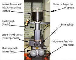
The hyperspectral-imaging microscope system (HIMS) includes a hyperspectral microscope jointly developed by XenICs and Twente University for research work on light-emitting semiconductor structures in the infrared (IR) region (see Fig. 2). The microscope's lens is designed to work in the IR. A beamsplitter deflects about one-third of the emission to a laterally positioned CMOS camera, which serves as a tool to direct the microscope and select the surface portion of interest on the test object. The IR camera can be positioned on top of this, directly or together with a spectrograph.
The IR camera and its InGaAs sensor array are cooled by a water-cooled Peltier element. This offers at least two advantages: it works within the camera head without needing a fan. For the user, this lowers the vibration level. In addition, the camera itself is of lighter weight; after all, it is to be moved up to 25 mm across the test object by a microfeed with stepping motor to do a line scan. In fact, to be more flexible in its applications, the hyperspectral microscope is constructed as a movable unit. In its base, it carries the PC for the control and evaluation programs, as well as a chiller for the camera's water cooling.
The spectrograph (from Specim; Oulu, Finland) operates in transmission mode and does not require any movable mechanical parts. The dispersion element is a grating with high permeability (more than 50%) and a spectral resolution of 5 nm in the near-IR (NIR) region from 900 to 1700 nm. The IR lens of the microscope projects the surface to be measured onto the spectrograph, which performs a spectral dispersion of the impending light and projects the spatial axis as well as the perpendicular spectral axis via a coupling lens onto a NIR surface sensor.
XenICs is one of the few vendors specializing in NIR image capture and cameras for extremely diverse applications. The software-configurable NIR digital camera used in the HIMS, with its InGaAs focal-plane array, covers the standard wavelength area from 900 to 1700 nm. Pixel pitch is 30 µm at a pixel availability of more than 98%.
One of the development goals of the hyperspectral microscope was to achieve the same geometric resolution in both x and y directions. While pixel pitch determines x-axis resolution, the resolution of the y-axis is tracked by appropriately driving the microfeed step motor. The camera head communicates with a PC via standard data interface such as USB 2.0 for the control signals, and Camera Link or a parallel LVDS bus for the 14-bit image data. The camera is quickly integrated to different application environments through its standard lens C-mount and spectrometer mount.
A multitude of functions
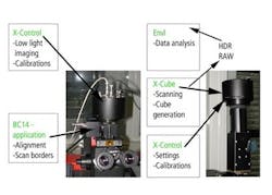
The hyperspectral microscope is universally applicable in the examination of light-emitting semiconductors. It can be used in two measurement setups: one for direct surface capture and one for spectral analysis through the spectrograph (see Fig. 3). Software support in the case of light-emitters is provided by the X-Control graphical user interface, which comes with every camera. X-Control enables direct access to various camera settings, such as integration time or operating temperature. It also contains software tools such as two-point uniformity correction and bad-pixel replacement.
The laterally mounted CMOS camera allows the user to adjust and select the scan area for hyperspectral examination, which is done by a parameter definition. In the configuration shown on the right of Fig. 3, this process is very time-consuming. Here, too, X-Control is used for parameter adjustment whereas the X-Cube software tool controls the scan procedure und generates a three-dimensional data set of x, y, and spectral coordinates in *.RAW format. Finally the evaluation is performed within ENVI (environment for visualizing images), which contains finely tuned and proven programs as well as thousands of options.
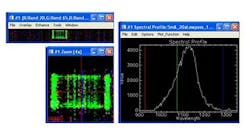
One of the first captures performed by the hyperspectral microscope is a spectral analysis of the LED structure in Fig. 1, in the ENVI environment--first in three-channel false-color rendering, followed by fourfold magnification and selection of an appropriate analysis coordinate, and finally the spectrum profile (see Fig. 4). It is clearly visible that a three-channel multispectral analysis has only marginal meaning.
This examination principle is applicable to all materials and structures that fit under a microscope and are in any way marked and identified by specific spectral information. The method's quick and meaningful results can substantially contribute to a shortening of the design procedure of new product introductions and thus accelerate the pace of LED innovation.
BOB GRIETENS is CEO of XenICs (Leuven, Belgium) and JISK HOLLEMAN is an associate professor in the electrical engineering department at the University of Twente (Enschede, the Netherlands); e-mail: [email protected].


