Light-activated microwave method improves semiconductor carrier-lifetime measurement

May 1, 2019
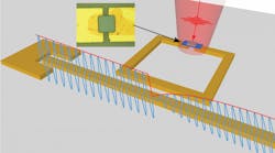
A circuit analog of time-resolved microwave reflectance using an RF-concentrating resonator amplifies the response to optical excitation of a small volume of optoelectronic material under test for ultrasensitive carrier lifetime measurements.

Measurement of electron carrier lifetimes in semiconductor materials typically uses time-resolved photoluminescence or direct-current photoconductive-decay methods. The former method suffers from poor accuracy for small samples and requires bulky collection optics and a detector tailored to the sample’s emission wavelength, whereas the latter technique requires fabrication of custom ohmic contacts and is not feasible for certain organic or 2D materials.

An alternative method spearheaded by the University of Texas at Austin uses a variation of time-resolved microwave reflectance (TMR) to instead probe the change in RF conductivity over time upon optical excitation (rather than depending on PL emission and, hence, eliminating the need for optics/detectors or ohmic contacts). The team designed a microstrip split-ring resonator (SRR) that strongly localizes the RF field interacting with a photoexcited material under test, enabling electrical readout of carrier dynamics with five orders of magnitude better measurement sensitivity and with incident optical intensity values as low as 35 fJ on material samples as small as 24 × 24 µm.

By placing a small volume of material in the microwave SRR circuit, the microwave signal is amplified when illuminated and easily read on an oscilloscope with higher accuracy and at lower cost than other methods. Carrier lifetime measurements define the overall optical quality of a semiconductor or other optoelectronic material, dictating the range of applications for which that material is suited. Reference: S. Dev et al., Nat. Commun., 10, 1625 (Apr. 9, 2019).
About the Author

Gail Overton | Senior Editor (2004-2020)

Gail has more than 30 years of engineering, marketing, product management, and editorial experience in the photonics and optical communications industry. Before joining the staff at Laser Focus World in 2004, she held many product management and product marketing roles in the fiber-optics industry, most notably at Hughes (El Segundo, CA), GTE Labs (Waltham, MA), Corning (Corning, NY), Photon Kinetics (Beaverton, OR), and Newport Corporation (Irvine, CA). During her marketing career, Gail published articles in WDM Solutions and Sensors magazine and traveled internationally to conduct product and sales training. Gail received her BS degree in physics, with an emphasis in optics, from San Diego State University in San Diego, CA in May 1986.

Sponsored Recommendations

Request a quote: Micro 3D Printed Part or microArch micro-precision 3D printers

April 11, 2024
See the results for yourself! We'll print a benchmark part so that you can assess our quality. Just send us your file and we'll get to work.

Request a Micro 3D Printed Benchmark Part: Send us your file.

April 11, 2024
See the results for yourself! We'll print a benchmark part so that you can assess our quality. Just send us your file and we'll get to work.

Request a free Micro 3D Printed sample part

April 11, 2024
The best way to understand the part quality we can achieve is by seeing it first-hand. Request a free 3D printed high-precision sample part.

How to Tune Servo Systems: The Basics

April 10, 2024
Learn how to tune a servo system using frequency-based tools to meet system specifications by watching our webinar!

Voice your opinion!

To join the conversation, and become an exclusive member of Laser Focus World, create an account today!