Because its probe and reference beams follow the same path, a common-path interferometer can measure changes in optical phase while being mostly unaffected by ambient variations such as air turbulence. This sort of instrument is useful for precision motion control, as well as for measuring vibrations, surface profiles, variations in refractive index, and other attributes. Phase-shifting versions of common-path interferometers, either temporal (sequential phase steps) or spatial (three or four simultaneous side-by-side beams, each one phase-shifted by a different amount) provide a particularly good signal.
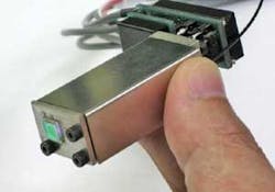
Two researchers at Hitachi (Yokohama, Japan), Toshihiko Nakata and Masahiro Watanabe, have developed a spatial phase-shifting common-path interferometer that is built around photonic-crystal polarizers (PCPs), making the design compact and simple, and many of its components monolithic.1 The instrument, which is about the size of a man’s thumb, has another advantage: the probe beam makes two round-trips between the reference mirror and the sample instead of the usual single round-trip, doubling the phase change and thus the sensitivity.
PCP mirror and phase-shifter
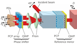
In the interferometer, a source beam with a 45° polarization is directed off a beamsplitter to a PCP reference mirror, which splits the beam into orthogonally polarized reference and probe beams and reflects the reference beam back toward the phase-shifter and detectors (see figure). The probe beam goes through a quarter-wave plate (QWP), bounces off the sample twice and the PCP once, and is then transmitted back through the PCP to the phase-shifter, recombining with the reference beam.The PCPs consist of 2-D subwavelength structures that are made by depositing two different kinds of dielectric films in alternating layers over a subwavelength grating, which gives the dielectric stack a triangular corrugation. The PCP variables, which can be tailored to suit different wavelengths, are the grating pitch, the stacking period, and the number of layers.
Low noise
The researchers built a prototype interferometer module measuring only 20 × 50 × 14 mm in size, with light supplied via single-mode polarization-maintaining fiber from a He-Ne laser. Its phase-shifter contains four PCPs, each 2 × 2 mm, all monolithically integrated on a silica substrate, according to Nakata.
When tested with a stage scanned linearly over a 200 nm range, the device produced four signals mutually shifted by π/2 and varying with a 158.2 nm period, confirming the device’s doubled phase change when compared to conventional interferometers. A 1 nm scan produced displacement data showing that the displacement noise level of the interferometer was less than 40 pm.
The researchers believe the instrument is well suited for position and displacement measurements on the millimeter scale, such as those for microelectromechanical systems and scanning-probe microscopes, and note that it could also be used in techniques that measure two-dimensional sample profiles, such as a pixelated phase-mask scheme.
REFERENCE
- T. Nakata and M. Watanabe, Applied Optics 48(7) (March 1, 2009).


