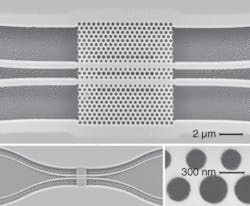
Most optical switches operate by shutting light on or off, or by directing light between two different ports of the device through inducing a refractive-index change or phase shift between the two ports. Because these refractive-index changes are typically small, the result is often a very long-path-length device with the switching region being more than 150 µm in length. Using a silicon directional coupler within closely spaced photonic-crystal waveguide structures, researchers at the University of St. Andrews (Fife, Scotland) took advantage of slow-light enhancement within the device to create an optical switch that is 36 times shorter than a conventional device with the same refractive-index change.
Switching in a directional-coupler device of length L occurs when the relative path length of the light changes by half a wavelength—a phase shift of π—and is brought about by a refractive-index change Δn defined by ΔnL = λ/2. By engineering the hole structure within the photonic-crystal material surrounding the coupler waveguides, the dispersion of the central coupling region can be controlled (see figure). For the device fabricated by the research team, three different hole radii of 0.30a, 0.34a, and 0.39a (a = lattice period of 430 nm) were used to effect switching in an L = 5.2 µm device. The refractive-index change is 0.0042, meaning that the ΔnL product is 22 nm, or 36 times smaller than a conventional device with wavelength 1574 nm, with a ΔnL product of λ/2 or 787 nm.
Slow-light enhancement
The key design feature responsible for the ultracompact switch is slow-light enhancement, in which one of the two supermodes of the directional coupler has a slow group velocity. The slow group velocity of the light in the device effectively increases the optical path length of the waveguides, thereby increasing the interaction between them for the same physical length. This increased interaction allows the switching length to be dramatically reduced.
Electron-beam lithography was used to fabricate the devices, controlling hole size to an accuracy of 1%.
In a proof-of-principle experiment, a broadband light-emitting-diode (LED) source illuminated one of the input ports of the device. Switching was demonstrated by using the thermo-optic effect (heating the stage on which the device is mounted to induce an index change). At near-infrared wavelengths, silicon will produce a refractive-index change of 0.00018 per degree Kelvin, sufficient for switching in this device. Input light was switched between the two ports by alternating the temperature between 23°C and 45°C. Switching at a wavelength of 1575 nm occurred with a discrimination ratio exceeding 30 dB for an index change as small as 0.0042.
Although the bandwidth of this switch is limited to 1.2 nm, it can accommodate 100 GHz optical signals. In addition, the flexible design allows customization of the dispersion curves to modify the operating wavelength.
Researcher Thomas Krauss says, “At the moment, optical switches tend to be millimeters in size. It is difficult to state which is the smallest optical switch ever made, but this is definitely one of them.” Krauss predicts that a matrix of such switches will one day be used in integrated optical networks. “The whole point of going smaller is so that you can make the switch matrix small.”
REFERENCE
1. D.M. Beggs et al., Optics Lett. 33(2) 147 (Jan. 15, 2008).

