Photonic-bandgap materials such as photonic crystals are important for their ability to manipulate photons. Much of the effort has been concentrated in the three-dimensional (3-D) manipulation of photons through the engineering of defects with the photonic-crystal (PC) material. Such defects disrupt the PC lattice periodicity and create a state for forbidden bandgap frequencies to be routed or manipulated toward the development of embedded resonant cavities, waveguides, and other optoelectronic structures. In fact, a well-engineered 3-D photonic crystal could form the basis of a 3-D optical network in similar fashion to the technology described in, “Polysilicon resonates toward CMOS-compatible 3-D networks.”
Researchers at the University of Illinois at Urbana-Champaign (Urbana, IL) are working to improve the engineering of defects in PCs and have created high-quality defects within a silicon inverse opal crystal, demonstrating the first waveguiding of near-infrared light around sharp bends within this material.1 This feat is essentially achieved through two-photon polymerization (TPP) within a self-assembled silica colloidal opal followed by a high-index replication step and removal of the opal template with acid to create the defect. Researchers from BASF Aktiengesellschaft (Ludwigshafen, Germany), Laser Center Hannover (Hannover, Germany), and Thales (Paris, France)-working in the European consortium NewTon-are also using a similar methodology: spaces between polymer spherical particles in a crystal lattice are filled with silicon and then the polymer particles are “burned” out of the lattice creating a stable structure that is a mirror image of the original crystal. Crystals of this type could be used as components for an all-optical routing processor in telecommunications.2
Etching process
The Urbana-Champaign technology begins with the growth of an artifical opal, a periodic array of silica spheres self-assembled into a face-centered-cubic lattice on a double-side polished silicon substrate from precalcined silica spheres (725 to 925 nm in diameter) using a modified vertical deposition technique. A thin film of amorphous alumina is then grown around the spheres through atomic-layer deposition in order to enhance the mechanical stability of the structure and provide control over the degree of interpenetration between the spheres, facilitating the etching of the silica colloids in the final step.
Next, polymer features are embedded within the colloidal crystal using TPP. A fluorescent dye is added to the polymer to facilitate real-time observation during the TPP process and registration of the features within the underlying crystal lattice, easily achieving 500 nm linewidths and less than 100 nm edge resolutions. This colloidal photonic crystal with embedded TPP features is then infiltrated with an amorphous silicon layer through chemical vapor deposition. The structure is then etched through a combination of reactive ion, ozone, and chemical processes to remove the silicon overlay, oxides, and polymer to leave behind the silicon crystal with embedded structure.
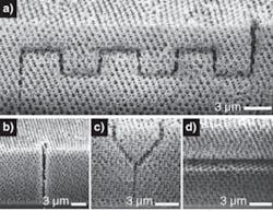
Using this technique, the research team is able to fabricate high-quality cavities, waveguides, splitters, and even more complex features within the silicon opal (see figure). To demonstrate the functionality of the embedded devices, 1480 nm near-infrared light was sent through a waveguide containing two 90° right-angle turns. When light with frequencies outside this photonic bandgap was used to collect transmission micrographs from the double-bend waveguides, it could not be differentiated from the background, indicating that guided modes exist within the embedded features only for frequencies within the photonic bandgap. This initial demonstration should encourage further efforts in the development of 3-D photonic crystals for telecom and optoelectronic applications.
“We believe this work represents only the starting point of what can be accomplished with features embedded in 3-D photonic-bandgap materials,” says Paul Braun, associate professor of Materials Science and Engineering at the University of Illinois at Urbana-Champaign. “Through careful feature design, functionalization of the features with optically active materials such as quantum dots, and coupling of features to active on-chip elements, significant advances in optical materials and devices will be enabled.”
REFERENCES
1. S.A. Rinne, F. Garcia-Santamaria, and P.V. Braun, Nature Photonics 2(1) 52 (2008).
2. BASF Aktiengesellschaft, “3-D Photonic Crystals Will Revolutionize Telecommunications,” Science Daily online (Nov. 21, 2007).

