What is the biggest and most influential technological change to come along in the past 50 years, and one of the few that deserves to be called a revolution? Is it the introduction of the Sony Walkman? Whole-wheat spaghetti? The “Baby on Board” car sign?
No, few would disagree that it is the introduction of digital technology into our daily lives, in the form of PCs and the Internet–as well as ATMs, cell phones, DVDs, and so forth. While many trace the roots of this revolution back to the fabrication of the first integrated circuits by Jack Kilby of Texas Instruments and Robert Noyce of Fairchild Semiconductor, photonic technology has been insinuating itself into the digital era from the start. Optical lithography is the preferred method of patterning computer chips; once capable of producing features no smaller than tens of microns in size, it is now used for volume production of chips with 45 nm features. Fiber-optic communications, digital cameras, diode lasers for printers and CD players–all contribute to our digitally driven world.
And now photonics is aiming right at the core. Multicore processor chips–which are the semiconductor industry’s latest approach to maintaining Moore’s Law (a doubling of the number of transistors on a computer chip every two years)–will require communications capacities beyond what electronics can provide. Ultimately interchip, and then intrachip, optical interconnects will enable years more growth in computer speed and capacity, leading to a degree of networking in our daily lives the likes of which we now merely guess about.
In this and many other ways, scientists and engineers are exploiting the photon for practical use, as well as for the sake of knowledge. From the creation of the largest combined primary and tertiary telescope mirror ever, to the use of light (and sound) to detect explosives, and to designs for small, quickly focusing lenses for digital cameras, this past year has seen more than its share of achievements in photonics–some of them not well-publicized.
Optics, macro and micro
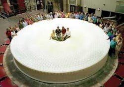
One of the world’s largest single telescope mirrors, and the largest monolithic combination of two mirrors, is the 8.4 m mirror for the Large Synoptic Survey Telescope (LSST), to be located at Cerro Pachon, Chile. The 26-ton lightweighted disk of Ohara E6 borosilicate glass emerged this year, cooled, from its spin-casting oven at the University of Arizona’s Steward Observatory Mirror Lab (Tucson, AZ), ready to be ground and polished (see Fig. 1). With a focal length of 9.9 m, the completed telescope will survey a 20,000-degree2 area of sky 1000 times over 10 years in six visible bands, producing 30 Tbytes per night of data. The site will require 200 Pbytes (2 × 1017 bytes) of data storage.
Toward the other end of the size scale is a 0.5-mm-diameter laser-scanning mirror fabricated by researchers at Toyota Technological Institute (Nagoya, Japan) and Tohoku University (Sendai, Japan), which combats the problem most scanning mirrors have: too much mass. The mirror, which is flat to λ/10 in visible light, consists of a polycrystalline silicon (Si) membrane across a rigid crystalline Si ring; the membrane is under 600 MPa of tension.1 The crystallization-induced stress is independent of temperature, making the flatness stable over a wide temperature range even when the mirror is coated with metal.
Small variable-focus liquid lenses are being more widely developed, and have made their entry into the marketplace. Shenzhen Akkord Electronics (Shenzhen City, China) is now selling a cheap ($20) webcam that has a liquid lens made by Varioptic (Lyon, France), which has been working on the technology for years (see www.laserfocusworld.com/articles/224009). Although the ability of the lens to shift focus in 0.02 seconds is likely not much of an advantage while imaging a sitting Web surfer, the lens’ low cost (which can only go lower as production is ramped up) most certainly is.
In a well-publicized announcement, researchers at Rensselaer Polytechnic Institute (Troy, NY) described their version of a liquid lens: a droplet of water overfilling a hole in a hydrophobic plate and oscillating at its natural frequency of 100 Hz (see www.laserfocusworld.com/articles/343739). Because the droplet is cycling through a range of focal lengths many times a second, the optical system’s imaging camera need only snap a picture at the right instant to take advantage of a particular focal length. Much less publicized was the equally significant deposition of a polymer thin film and a conductive transparent silver film directly onto a liquid droplet by scientists at the University of Tokyo (Tokyo, Japan), creating an encapsulated, electrostatically focused microlens.2 Various versions with diameters from 20 µm up to a whopping 30 mm were created; the focal length of a prototype 1-mm-diameter lens could be varied down to 20% of its initial 3.7 mm value.
Peekaboo
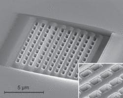
Optical metamaterials appeal to the geek in many of us because of what the materials can theoretically do: not only could their odd properties result in some very unusual optical systems, but someday they may make us invisible (if you believe the popular press). In reality, researchers at the University of California, Berkeley, have demonstrated a 3-D negative refractive index in an optical metamaterial made of many fishnet metal/dielectric layers, by fabricating a prism of the material about 10 µm in size (see Fig. 2).3 When laser light was shone on the prism and tuned from a 1.2 to 1.775 µm, the refractive index decreased from 0.65 to -1.35, as revealed by the refraction angles. One important property of the material is its transparency, which is high in comparison to other metamaterials, thus allowing optical elements to be fabricated (however small).While theoreticians have come up with certain optical-metamaterial configurations that could serve as cloaking devices (“invisibility cloaks”), and scientists have actually constructed small cloaking devices that work at microwave frequencies, the rapid advances in 3-D optical metamaterials have caused some scientists to state that a real-life invisibility cloak may be only a few years away. Such a shield might, when fabricated, manage to cloak a dusk speck at a single wavelength; however, the popular press has translated such a device into a human-size cloak–which would be valuable indeed, especially if you could zip it up against the wind.
Now, as an antidote to the metamaterial invisibility cloak, three researchers from Shanghai Jiao Tong University (Shanghai, China) have introduced–the anti-cloak.4 Such an apparatus, which would also be made of an optical metamaterial and would have to be placed inside the invisibility cloak, would partially cancel the cloak’s invisibility properties, revealing the speck of dust–or the person–inside. And rumors are flying of an even-more-effective anti-cloaking approach, which takes the form of a handheld device and is colloquially referred to as a can of spray paint.
Making light
New light sources of many types and wavelengths are plentiful this year. At the short end of the spectrum, the Thomson-Radiated Extreme X-ray Source (T-REX) at Lawrence Livermore National Laboratory (Livermore, CA) has produced gamma-ray photons with an energy of 0.776 MeV (a wavelength of 0.0016 nm) at a brightness of 1017 photons/s/mm2/mrad2/0.1% bandwidth, which is brighter than advanced synchrotron sources by six to nine orders of magnitude. In the T-REX, 263 nm fourth-harmonic laser light strikes a cathode to produce electron bunches, which are then accelerated to relativistic speeds; these electrons are fired head on at a pulse of 355 nm (frequency-tripled) photons, which scatter off the electrons to generate gamma rays. T-REX can be used for isotope-specific medical and industrial imaging, as well as detection of hidden enriched uranium.
One of the highlights this year was the creation of 80-attosecond pulses of light by researchers at the Max-Planck-Institut für Quantenoptik (MPQ; Garching, Germany), the Ludwig-Maxmilians-Universität (also in Garching), and the Lawrence Berkeley National Laboratory (Berkeley, CA); the pulses, which are broadband with a peak in the extreme-ultraviolet range, will serve to probe the hyperfast interactions of electrons within atoms (see www.laserfocusworld.com/articles/335960). They are created by subjecting a jet of neon gas with a sub-1.5-cycle ultrafast laser pulse, briefly ionizing it with the pulse’s peak cycle. Eleftherios Goulielmakis, the head researcher, believes that zeptosecond (10-21 s)-scale pulses might be possible in the future, permitting the probing of atomic nuclei.
Even when it comes to high-power military laser systems, simplicity can be very effective. Much work is going into developing a 100-kw-class laser taking the form of a single large emitter; however, researchers at the Naval Research Laboratory (NRL; Washington, D.C.) and Icarus Research (Bethesda, MD) are pursuing an alternate technique, incoherent beam combining, in which many lower-power laser beams are combined, basically by aiming them all at the same target (see www.laserfocusworld.com/articles/334128). Such an approach avoids the complexities of coherent or spectral beam combining, while in some cases producing an almost diffraction-limited focal spot on the target. In a proof-of-concept experiment, the NRL combined four fiber lasers with a total output of 6.2 kW and a transmitted power of 3 kW, delivering 2.8 kW to a 10-cm-radius target 1.2 km away. Ultimately, a 500 kW system with 100 fiber lasers (5 kW/fiber) would function using a beam-directing mirror only 40 cm in radius.
While ytterbium-doped fiber lasers can produce many kilowatts of optical power, their output is not eye-safe. By shifting laser output to around 2 µm, this safety problem could be at least mitigated, resulting in an “eye-safer” IR fiber laser–one whose wavelength could not penetrate the eye and destroy the retina (although, as with any high-power laser, its light could still burn the skin or cornea). Engineers at Q-Peak (Bedford, MA) have built such fiber lasers, of thulium-doped silica–one with an output of 301 W and a beam quality of M2 = 1.2, and another with a multimode output of 885 W and a 50.7% efficiency.5 They aim next for an all-fiber-coupled design.
The rise of fiber lasers, first to practicality and then to very high powers, has been dramatic. But can their output power always be made higher? No, say researchers at Lawrence Livermore National Laboratory, who did a theoretical analysis of diffraction-limited single-fiber lasers to determine their physical limits (see www.laserfocusworld.com/articles/342651). They considered two cases: broadband, for which stimulated Brillouin scattering (SBS) need not be considered, and narrowband, for which SBS is relevant, and got fundamental upper-power limits of 36.6 kW and 1.86 kW, respectively. The researchers note that their derivation was what was most important, as further technological improvements–for example, fibers able to suppress SBS–could alter the starting assumptions.
Terahertz radiation occupies that nebulous wavelength region between light (manipulated by optics) and radio waves (manipulated by antennas and electronics). Taking advantage of this, two researchers at RIKEN (Sendai, Japan) have created a beam steerer that potentially offers rapid aiming of a terahertz beam over a ±90° range–useful for short-range communications (see www.laserfocusworld.com/articles/338722). The terahertz beam is produced by illuminating a strip-line photoconductive antenna with two separate beams split from an 803-nm-emitting ultrafast Ti:sapphire laser. Changing the angle between the laser beams by a very small amount (much less than a degree, which could potentially be done by an electro-optic beam-steerer) changes the terahertz-beam angle by a large amount. As an added degree of control, changing the lateral spacing between the laser beams changes the terahertz frequency.
Keeping up with Moore’s Law
Optical interconnects within a computer can be divided into three types: rack level (rack-to-rack optics), board level (on-card interconnects), and chip level (connecting processors together). In June of this year, IBM Research (Yorktown Heights, NY) announced that a supercomputer that the company’s engineers had programmed and built at the Lawrence Livermore National Laboratory, called Roadrunner, was the first ever to break the petaflop barrier (a quintillion floating-point operations per second); indispensable to the computer’s record-breaking performance was its active cable fiber optics. In another development, Luxtera (Carlsbad, CA) this year introduced a monolithic 40 Gbit/s optoelectronic optical active cable–the first integrated (optical and electronic on CMOS) interconnect to go into volume production.
Board-level optical interconnects have also been advanced by IBM, which has fabricated what it calls a Terabus link–two transceiver optomodules on a card with integrated multimode polymer waveguides; the optomodules can transmit 160 Gbit/s both ways (16 channels at 10 Gbit/s each).6 In the next five years or so, such board-level optics should move out of the laboratory and into real systems.
On-chip optical interconnects are the furthest away from practicality: their disparate elements are at the moment either in the first-prototype, the conceptual, or the not-yet-figured-out stage, and have years to go before being assembled into a complete system that connects processors together into a nicely functioning mesh. However, some of the optical technology useful for board-to-board or chip-to-chip interconnects could eventually be used for on-chip communication.
Researchers at Intel (Santa Clara, CA) have developed hybrid III-V semiconductor tunable lasers on Si; a quantum-well-intermixing process allows differing bandgaps to be created for various parts of the device, such as the mirrors, the gain region, the phase region, and the backside absorber (see www.laserfocusworld.com/articles/343731). The light from the laser is evanescently coupled into silicon dioxide (SiO2) waveguides on the Si chip. The researchers have also integrated tunable lasers with electroabsorption modulators, and see such components as forming part of a low-latency wavelength-division-multiplexing intracomputer data-communications system. Intel is developing a variety of photodetectors to use with its tunable lasers, including silicon-germanium (Si-Ge) avalanche photodetectors, p-i-n photodetectors, and hybrid photodetectors fabricated with the same technique as the company used for its lasers.
A group at the Massachusetts Institute of Technology has integrated gallium aluminum arsenide vertical-cavity surface-emitting lasers (VCSELs), in the form of 55 µm stand-alone “pills,” into Si CMOS IC chips (see www.laserfocusworld.com/articles/342658). The pills are bonded into etched recesses in the chip, which are replanarized, then patterned with electrical interconnects; the VCSELs’ threshold currents are the same before and after integration.
And at Cornell and Columbia Universities (Ithaca and New York, NY), researchers demonstrated a microring-resonator-based single-wavelength Si optical router that routes four inputs to four outputs with no overlap of signals (which, of course, is significant for single-wavelength routing because spectral beamsplitting cannot be used to separate signal paths). The microrings are thermally tuned with nichrome heating rings that sit atop the resonators (see www.laserfocusworld.com/articles/343738).
The Cornell group has demonstrated other components essential for dense on-chip electronic and photonic integration. In one example, a resonant electro-optic microring modulator on Si maintains a 1 Gbit/s modulation speed over a wide (15 K) temperature swing; this is achieved by varying the bias current through the modulator, thus controlling the device’s temperature.7 In another, a Ge thin-film single-crystal photodetector is integrated onto a submicron waveguide on a silicon-on-insulator (SOI) wafer in a low-temperature process (less than 400°C) that is compatible with CMOS microelectronic processing; the detector has a dark current of 100 nA and an efficiency of greater than 90%.8 The process consisted of bonding the implanted Ge wafer and the patterned SOI wafer together at room temperature under pressure; after annealing at 100°C, the temperature was raised to 400°C, causing enough in-plane stress to split a thin Ge film from the bulk Ge wafer. The responsivity reached 0.44 A/W at 1527 nm; with some improvements to the detector, its speed is expected to reach 40 GHz and above.
The development of viable on-chip optical-interconnect technology was given a boost this year by the Defense Advanced Research Projects Agency, which awarded Sun Microsystems (Santa Clara, CA) a $44 million contract to develop optical interconnects for future multiprocessor computer chips. Sun will work with Luxtera and Kotura (Monterey Park, CA), along with a number of universities, to develop what it calls “macrochips”–which will contain hundreds of processing cores connected with optics. In this way, Moore’s Law will (we hope) remain in force for many years to come.
Significant others
Innovations of all sorts in photonics made their appearance this year; most likely, no two people in the field would pick the same list of favorites. As always, some advances are for the sake of knowledge, while others carry the aura of practicality. An example of the latter is a laser-based device developed at Oak Ridge National Laboratory (ORNL; Oak Ridge, TN) that relies on photoacoustic spectroscopy to detect very small amounts of explosives from as far away as 20 m (see www.laserfocusworld.com/articles/338723). While photoacoustic spectroscopy is not a new technique, the ORNL device improves on its sensitivity. A pulsed quantum-cascade laser emits 9.5 µm light that is aimed at the target; reflected and scattered light is focused onto a quartz-crystal tuning fork with a Q factor of 10,000. The researchers tested for TNT and other explosives, detecting surface concentrations of only 100 ng/cm2. Increasing the number of lasers will enable the stand-off distance to be increased to 100 m.
Optical storage within a DVD-size disk has reached the 1 Tbyte level, as demonstrated by scientists at Call/Recall (San Diego, CA) and the University of California, Irvine.9 The write-once read-many (WORM) medium consists of a dye-precursor and a light-sensitive photoacid generator dispersed in a polymethylmethacrylate host. Two-photon absorption of 532 nm light focused with a 1.0-numerical-aperture lens creates the recorded bits, which exist in 200 layers of 5 Gbytes each. The bits are read by making them fluoresce with 650 nm light and detecting the emission with optics and a photomultiplier. The WORM data can be stored for years without decay. The researchers have also done test recordings with a 405 nm laser diode and anticipate future 5 Tbyte disk capacities.
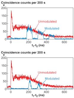
Ultrafast-laser-pumped fiber white-light supercontinuum sources, developed at the University of Bath (Bath, England) and commercialized by Fianium (Southampton, England), have gained output in the blue (see www.laserfocusworld.com/articles/343745). New photonic-crystal fiber designs that increase the air-filling fraction have pushed the short-wavelength-edge of the supercontinuum spectrum, which was previously at about 450 nm, all the way to 380 nm. The output of these sources now ranges from 2400 nm all the way to the near UV, making them useful for industrial and biomedical applications that require a true white-light spectrum. Fianium is now leading a consortium (which includes the University of Bath and Edinburgh Instruments) that aims to push the spectrum’s short-wavelength edge down to 300 nm.And, in a development that may seem as if it’s just for the sake of science but in fact has practical applications, scientists at Stanford University (Stanford, CA) have created single photons with arbitrary temporal waveforms–for example, a lone photon whose waveform consists of three separated square pulses (with zero waveform height between the pulses).11 The researchers first generate a pair of photons, Stokes and anti-Stokes, from rubidium atoms in a magneto-optical trap (MOT); the anti-Stokes photon is traveling slowly due to the electromagnetically induced transparency in the MOT. When the Stokes photon is detected, it signals an electro-optic modulator to shape the waveform of the anti-Stokes photon (see Fig. 5). The resulting waveform is observed by measuring many time-correlated single photons, counting the number of coincidences per unit of time. In one practical use of the technique, a photon can be shaped to have a time-reversed exponential decay that enables the photon to optimally enter a Fabry-Perot cavity.
REFERENCES
- M. Sasaki et al., J. Opt. A: Pure Appl. Opt. 10, 044004 (2008).
- N. Binh-Khiem et al., Appl. Phys. Lett. 93, 124101 (2008).
- J. Valentine et al., OSA CLEO/QELS 2008 postdeadline sessions, QPDB2.
- H. Chen et al., Optics Express 16, 14603 (Sept. 15, 2008).
- P. Moulton, SPRC 2008 Annual Symp.”
- J. Kash, SPRC 2008 Annual Symp.
- S. Manipatruni et al., Optics Lett. 33, 2185, (Oct. 1, 2008).
- L. Chen et al., Optics Express 16, 11513 (July 21, 2008).
- E. Walker et al., Appl. Optics 47, 4133 (Aug. 1, 2008).
- P. Choi et al., Science 322, 442 (Oct. 17, 2008).
- P. Kolchin et al., OSA CLEO/QELS 2008 postdeadline sessions, QPDA3.


