An international team of researchers has demonstrated a tunable nanophotonic source based on free electrons passing through a metal/dielectric stack. The approach could lead to widely tunable chip-scale sources for display technologies, nanophotonic and plasmonic circuits, and sensor applications.
The theory behind the “light well,” as the team calls it, is equivalent to that behind the free-electron laser (FEL)—the most widely tunable light source available. In an FEL, relativistic electron beams pass through an array of oppositely oriented magnets, producing synchrotron radiation as they go.
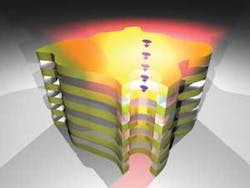
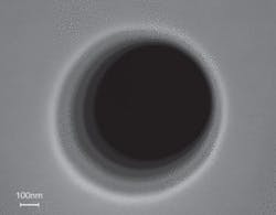
The light well produces incoherent near-IR photons as free electrons are accelerated by an applied field through a hole milled in an alternating stack of metal and dielectric plates. The work is a direct offshoot of the group’s expertise in plasmon generation.1
“Our group was the first to demonstrate that plasmons can be generated on a metal surface by a beam of electrons and then decoupled into free space,” says Nikolay Zheludev, the University of Southampton (Southampton, England) professor who led the research. “Since then we were interested in generating light by electron beams in nanostructures and, naturally, in developing a tunable nanoscale light source with a free-electron pump.”
Voltage tunes wavelength
The periodic nature of the stack presents a regularly varying dielectric environment for the electrons, which in turn emit incoherently. Like an FEL, the source is tunable via changes in the acceleration voltage. Higher voltages lead to lower wavelengths, and higher electron-beam currents result in higher intensities of emitted light.The input electron beams resulted in emission with two peaks; beams focused outside the well entrance resulted in acceleration-voltage-independent emission at 650 nm. Beams focused just inside the well, near its wall, showed broad emission that could be tuned with acceleration voltage. The output from the prototype devices is on the order of a tenth of a nanowatt, but the efficiency of the process is still fairly low–on the order of 10-5 photons per electron injected.2
Zheludev says the group is working to optimize the generation process through design of the wells’ geometry–principally the shape of the hole and the number and materials comprising the layers. “Essentially you have to balance between the generation capability of the light and transmission capability of the hole,” he says.
While the group concedes that the emission is a complex function of material- and geometry-dependent processes that don’t fit neatly into a single analytical model, some parameters will be easy to adjust. The researchers anticipate that longer wells will result in narrower emission and higher efficiencies, and the prototypes’ near-IR emission wavelength could easily be changed by adjusting the periodicity of the metal/dielectric stacks.
The group’s stock-in-trade is surface plasmons—the researchers demonstrated plasmon switching at terahertz rates earlier this year. Ironically, however, the generation of surface plasmons is a significant loss in the wells and is another issue to address.
Possibilities for displays
Zheludev says that working with pulsed electron sources is also part of the group’s plan; he believes that with tighter control of losses and higher drive currents, the wells could be made to achieve superradiant or even lasing modes. However, he says, there are plenty of applications for incoherent tunable sources on this scale. He points to surface-conduction electron-emitter display technology–“displays of zillions of small electron sources”–already on the market.
These are flat-panel displays comprising pixels in which nanoscale electron sources excite phosphors, each one like a tiny cathode-ray tube. Zheludev says that the light wells could be pumped by the electron sources and serve equally well as tunable emission sources for display technologies.
REFERENCES
- M. V. Bashevoy et al., Nano Lett. 6, p. 113 (2006).
- G. Adamo et al., Phys. Rev. Lett. in press; http://arxiv.org/abs/0907.2143.


