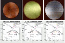
Inkjet printing is so good at positioning and meting out the right quantity of material that it can be used not just for producing documents, but in industry as well–for example, to fabricate solar cells or to create etch patterns for photodiode arrays. Now, scientists at Arizona State University (ASU; Tempe, AZ) and the University of Oulu (Oulun Yliopisto, Finland) are using the process to print quantum-dot LEDs (QDLEDs). Not only does inkjet printing conserve expensive QD-containing fluid; it also allows for the possibility of patterning full-color pixelated displays (although the printer that the scientists are using now can print only a single color at a time).1
Quantum-dot ink
In one example, quantum dots with a cadmium selenide core, zinc sulfide shell, and a capping organic ligand were obtained from Evident Technologies (Troy, NY) and used as received; the QDs were suspended in chlorobenzene to create ink. The substrate, a piece of glass precoated with the transparent conductor indium tin oxide (ITO), was coated with a 20 nm layer of poly-TPD, which was then cross-linked and served as the hole-transport layer.
Pixelated patterns of QDs with three different emission wavelengths–red, green, and blue–were printed in monochrome arrays on three different substrates, then coated with an electron-transport layer (TPBi) and a lithium fluoride/aluminum electrode (see figure). The ink fluid and the jetting properties of the printer (a Dimatix DMP 2800) were chosen and controlled to reduce variations in the thicknesses of the printed features.
The printed pixels were L-shaped, with a total area each of 19,600 µm2 (about 160 × 160 µm); spacing between each pixel was 80 µm. “The number of drops used per pixel, or subpixel, depends on the ink itself. Normally we use 5 to 25 drops per pixel, depending on ink,” notes Ghassan Jabbour, a professor at the School of Materials at ASU and the director of the ASU Advanced Photovoltaics Center.
Refining the process
To print the red, green, and blue pixels, the researchers had to optimize the drop registration, given the fact that the inkjet system could print only one color at a time. “Due to this limitation, the cartridge-change process creates registration misalignment, which needs to be addressed and checked each time a cartridge is changed,” says Jabbour. “We have done this beautifully.”
The resulting operating voltage is 10 to 15 V and the brightness is on the order of 300 cd/m2. “We are working on decreasing the drive voltage and increasing the brightness further,” says Jabbour.
Although the peak external quantum efficiency (EQE) of the first prototype reached only about 0.19% at 14.2 V, this low performance was not due to the inkjet process; for comparison, the researchers spin-coated a layer of QDs and measured its EQE to be even lower–about 0.15% at 20.7 V. Boosting the performance of the inkjet-printed QDLEDs could be achieved by washing the QDs repeatedly before they are incorporated into the ink, say the researchers.
Next: active-matrix
In addition to optimizing the device performance, the group is working on integration of the inkjet-printed pixels with an active-matrix backplane, according to Jabbour. If achieved, this would be a major step toward the appearance of pure red-green-blue full-color QD displays with an active layer manufactured as easily as one prints out a document.
REFERENCE
- H. M. Haverinen et al., Appl. Phys. Lett. 94, p. 073108 (2009).

