Designing photonic devices relies heavily on modeling their behavior with computational simulations. These simulations often require substantial computational resources and time, particularly when dealing with large structures like millimeter-scale geometries. This bottleneck impedes the pace of innovation and increases the time-to-market for new devices. However, the power of hardware-accelerated simulation offers a paradigm shift in how we approach photonic device design.
Leveraging advanced parallel computing architectures
In the rapidly evolving landscape of computational hardware, advanced parallel computing chips such as graphics processing units (GPUs), tensor processing units (TPUs), and field-programmable gate arrays (FPGAs) are experiencing unprecedented acceleration in performance. This surge is largely fueled by the burgeoning demand for artificial intelligence (AI) applications, a trend that shows no signs of abating. In fact, the pace of innovation is likely to accelerate even further. Concurrently, the field of computational electromagnetics offers a plethora of methodologies, each with its own set of advantages and limitations. Traditional approaches like the finite element method (FEM) and the boundary element method (BEM) often involve complex matrix inversion operations, rendering them less amenable to parallelization. However, there exists a subset of computational electromagnetics methods that are intrinsically well suited for parallel computing architectures. Time-domain methods, which employ explicit time-stepping algorithms, stand out in this regard. The most notable example is the finite difference time domain (FDTD) method. The FDTD algorithm is inherently parallelizable, making it an ideal candidate to leverage the computational prowess of modern parallel computing hardware.
By aligning the time-domain method with the capabilities of state-of-the-art parallel computing chips, we can unlock new dimensions of performance and efficiency. This synergy not only propels the field of computational electromagnetics forward, but also paves the way for more complex simulations and real-world applications. Next, we will see the power of the hardware-accelerated EM simulator in two case studies.
Case study 1: Polarization splitter rotator
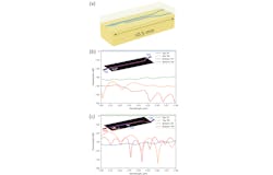
This case study focuses on a polarization splitter rotator (PSR),1 schematically illustrated in Figure 1a. This device employs a bi-level taper design to facilitate the transition of the input TM0 mode to the TE1 mode initially. Subsequently, the TE1 mode undergoes an adiabatic transition to the TE0 mode within the coupler region. Notably, the PSR spans over half a millimeter in length.
Traditionally, simulating this component using 3D FDTD methods would require tens of hours. However, leveraging the computational capabilities of Tidy3D, Flexcompute’s hardware-accelerated EM simulator, the simulation time is dramatically reduced to just 8 minutes in total for two separate runs—one with TE0 as the input mode and the other with TM0.
The results, displayed as the insets of Figure 1b and c, include field intensity distributions for both simulations. For the TE0 mode, the field remains in the TE0 state and propagates through the device to the ‘through port,’ without coupling to the ‘cross port.’ Conversely, for the TM0 mode, the field initially transitions to the TE1 mode and then adiabatically converts to the TE0 mode, directed towards the lower waveguide. More quantitatively, the mode conversion efficiencies are then plotted as functions of wavelength in Figure 1b and c. The results confirm that when the TE0 mode is launched, it transmits to the TE0 mode in the upper waveguide with minimal loss. Similarly, when the TM0 mode is launched, it converts to the TE0 mode in the lower waveguide, also with minimal loss.
The simulation validates the efficacy of the PSR, demonstrating both minimal loss and a wide operational bandwidth. This case study exemplifies how advanced parallel computing can significantly accelerate the simulation of complex millimeter-scale components in computational electromagnetics.
Case study 2: Adiabatic waveguide coupler
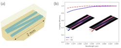
Next, let’s turn our attention to a thin film lithium niobate waveguide coupler that spans a length of 2 mm as schematically shown in Figure 2a.2 This device is designed to achieve adiabatic light transfer from one outer waveguide to another while minimizing the excitation of the middle waveguide. The adiabatic design offers several advantages, including exceptional fabrication tolerance, minimal mode and polarization sensitivity, and a broad operational bandwidth. This makes it compatible with both TE and TM modes, as well as fundamental and higher-order modes.
Coupling efficiency is plotted across a broad wavelength range from 1450 nm to 1650 nm in Figure 2b. Remarkably high-efficiency levels with a large bandwidth are observed. The simulation results of field intensity distributions for both TE0 and TM0 mode inputs are shown in the inset of Figure 2b. In both cases, light is successfully transferred from one outer waveguide to the other. Despite the device's large dimensions, the total simulation time was just 16 minutes in total for two simulations. This is noteworthy because traditional approaches often avoid using 3D FDTD for large-scale simulations due to the extended computational time required. Instead, approximation methods like 2D FDTD, beam propagation method, and Eigenmode expansion are commonly employed. However, these methods compromise accuracy, a trade-off that is not present when using 3D FDTD.
Closing remarks
These two case studies demonstrate the transformative impact of advanced parallel computing on the field of computational electromagnetics. Both examples benefit immensely from the capabilities of modern computational methods, offering compelling cases for their adoption in future designs.
REFERENCES
1. W. D. Sacher, T. Barwicz, B. J. F. Taylor, and J. K. S. Poon, Opt. Express, 22, 3777–3786 (2014).
2. Y.-X. Lin et al., Opt. Express, 29, 27362–27372 (2021).


