SILICON PHOTONICS: Silicon ‘expands’ to meet large-area applications

March 1, 2008
When we think about silicon photonics, we often picture a uniform, monolithic wafer of material.
(Courtesy Stanford University)
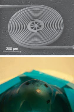
A scanning-electron micrograph shows a silicon island surrounded by coiled silicon wires (top). When the wires are uncoiled and attached to other silicon islands, the flexible array (bottom) can be used for large-area silicon-based applications including lower-cost solar cells and distributed sensor arrays.
When we think about silicon photonics, we often picture a uniform, monolithic wafer of material. But those images may soon be replaced by a web-like network of silicon islands surrounded by fine silicon wires. By pulling on the corners of silicon chips to unwind the coiled silicon wires fabricated next to them, researchers at Stanford University (Stanford, CA) can create flexible silicon arrays 50 times larger than the original silicon chips (see figure).1 These expandable arrays of prewired silicon chips conserve the amount of high-grade silicon used in a particular device, and can be applied to such large-area applications as light-emitting-diode (LED) displays, lower-cost solar cells, silicon-based distributed-sensor arrays, and curved focal-plane-detector arrays.

The expandable silicon is fabricated by using deep reactive-ion etching to create 30-µm-thick (although thicknesses up to 100 µm have been demonstrated), 200-µm-diameter circular silicon islands surrounded by 1.6-µm-thin spiral ribbons of silicon that act as springs. Each island can be a custom integrated circuit with unique electronics and electrical interconnects that run along the top of the coiled silicon wires to provide connectivity to other islands.

To uncoil the spiral ribbons, the devices are transferred to an electrostatic chuck, where stainless-steel probes manipulate pads at the corner of the coiled structures to expand the devices into an array. Once the desired size is achieved, the array is transferred to an adhesive surface. Although as many as 71 islands have been stretched to an array with an area 50 times larger than the uncoiled area of the structures, longer spiral springs could further extend this “expandable” network.

Surprisingly, the structures are quite robust; the coils can be fully extended multiple times without breaking and no delamination of the silicon dioxide coating used to overlay the final structures has been observed.

One unique product being explored by the research team is a curved focal-plane array that, by nature of its shape, eliminates many of the off-axis color mixing and image noise problems inherent in flat arrays. The curved array not only conforms to any shape (reducing the cost of imaging optics), but also offers single-crystal silicon performance in a low-cost, distributed configuration.

In early 2007, Stanford University researcher Peter Peumans founded NetCrystal (Mountain View, CA) to make solar panels using the expandable silicon arrays. He expects to make microconcentrator silicon solar arrays that are three times cheaper than comparable silicon solar panels. “The cost reductions come chiefly from a reduction in the cost of silicon and processing,” says Peumans. “The modules can be made flexible and can be readily integrated into building materials.”

“This is a platform technology that allows you to use monolithic silicon in entirely new applications such as smart materials,” says Kevin Huang, a Ph.D candidate working with Peumans. “Basically, it enables large-area electronics to benefit from the high performance and rapidly decreasing cost per function of CMOS technology.”

REFERENCE

1. K. Huang et al., IEDM 2007 Conf., Washington, D.C., session 9, paper 9.2 (December 2007).
About the Author

Gail Overton | Senior Editor (2004-2020)

Gail has more than 30 years of engineering, marketing, product management, and editorial experience in the photonics and optical communications industry. Before joining the staff at Laser Focus World in 2004, she held many product management and product marketing roles in the fiber-optics industry, most notably at Hughes (El Segundo, CA), GTE Labs (Waltham, MA), Corning (Corning, NY), Photon Kinetics (Beaverton, OR), and Newport Corporation (Irvine, CA). During her marketing career, Gail published articles in WDM Solutions and Sensors magazine and traveled internationally to conduct product and sales training. Gail received her BS degree in physics, with an emphasis in optics, from San Diego State University in San Diego, CA in May 1986.

Sponsored Recommendations

Request a quote: Micro 3D Printed Part or microArch micro-precision 3D printers

April 11, 2024
See the results for yourself! We'll print a benchmark part so that you can assess our quality. Just send us your file and we'll get to work.

Request a Micro 3D Printed Benchmark Part: Send us your file.

April 11, 2024
See the results for yourself! We'll print a benchmark part so that you can assess our quality. Just send us your file and we'll get to work.

Request a free Micro 3D Printed sample part

April 11, 2024
The best way to understand the part quality we can achieve is by seeing it first-hand. Request a free 3D printed high-precision sample part.

How to Tune Servo Systems: The Basics

April 10, 2024
Learn how to tune a servo system using frequency-based tools to meet system specifications by watching our webinar!

Voice your opinion!

To join the conversation, and become an exclusive member of Laser Focus World, create an account today!