Although many silicon photonic components have been developed toward the goal of on-chip optical networks (see www.laserfocusworld.com/articles/289409), progress has largely been based on silicon-on-insulator components in a single-layer, planar architecture. Researchers at Cornell University (Ithaca, NY) plan to break this bottleneck of limited real estate by focusing on vertical integration of multiple silicon layers. To date, wafer bonding, epitaxy, and other techniques have been used to demonstrate this three-dimensional (3‑D) architecture; however, none of these techniques is currently compatible with standard complementary metal-oxide semiconductor (CMOS) fabrication methods that could make the process cost-effective. But by using special thermal annealing steps, the Cornell researchers have demonstrated vertical coupling of polycrystalline silicon (polysilicon) photonic ring resonators to single-crystal silicon waveguides in an important step toward CMOS-compatible 3-D optical networks.1
First, a polysilicon ring resonator with radius of 40 µm coupled to a polysilicon waveguide is fabricated by growing a 2 µm thick silicon dioxide layer on a 4 in. silicon substrate and depositing a thin film of amorphous silicon. A two-step annealing process converts the amorphous silicon to polysilicon and removes defects from the crystalline regions. Electron-beam resist is spun on the polysilicon and the ring pattern is transferred to the substrate using e-beam lithography. A final silicon dioxide cladding layer is deposited by plasma-enhanced chemical vapor deposition. A quality factor of 20,000 and a maximum extinction ratio of 24 dB were measured for these polysilicon ring resonators. This is the highest quality factor reported to date in polysilicon optical resonators.
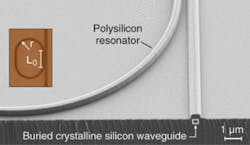
Next, these polysilicon resonators are vertically integrated with low-loss waveguides made of single-crystal silicon (although deposited amorphous silicon or silicon nitride films could be used and patterned into low-loss waveguides above or below the polysilicon rings). This vertical integration is achieved by patterning waveguides in a silicon-on-insulator substrate before topping these single-crystal silicon waveguides with the polysilicon ring-resonators using the fabrication process described previously (see figure). This resonator/waveguide system with a coupling region length of 3 µm has a measured quality factor of 4000-a factor-of-four better than previously demonstrated architectures. Placing the rings directly above the waveguides and including some additional polishing steps could further improve vertical separation and performance. In addition, annealing temperatures could be reduced by using excimer laser annealing.
For on-chip optical networks, the electrical and optical properties of polysilicon should be able to support ring resonator-based active devices including switches and modulators; in fact, the carrier concentration required in these polysilicon devices is comparable to that of gigahertz-speed electro-optic modulators in crystalline silicon. The ability to integrate layers of two different materials means that an optical network could make use of the electrical characteristics of polysilicon for active devices such as switches, while benefiting from the optical properties of amorphous silicon for long-distance on-chip light guiding. To the knowledge of the researchers, this is the first demonstration of a CMOS-compatible mixed-silicon optical system.
“The vertical integration of optical elements overcomes the traditional limitation of the relatively large sizes of optical elements on chip, enabling massive integration for high-density networks,” says Michal Lipson, Cornell University professor and researcher. “Polysilicon has been rarely used as an optical material due to its relatively poor optical properties, and the fact that such high-quality ring resonators were achieved is very encouraging.” Graduate research assistant Kyle Preston adds, “The next major step is lowering the processing temperature to achieve compatibility with back-end processing above the metal layers on a CMOS chip. This way, optical network functionality could be added on top of a chip after all the electronic processing is completed.”
REFERENCE
1. K. Preston, B. Schmidt, and M. Lipson, Optics Express 15 (25) 17283 (Dec. 10, 2007).

