STANISLAV SMIRNOV, KIRILL SOBOLEV, BRUCE TIRRI, ADEL JOOBEUR, AND RICK LEWIS
The need for high resolution is the main driver of an objective design for 45 nm critical-layer mask inspection. The necessary high resolution is achieved by a high-NA optical system and use of a 193 nm wavelength laser source over a small field. For patterned wafer-inspection optical designs, high resolution, as well as throughput requirements, push the design form to accommodate larger field sizes (in millimeter ranges).
Numerous challenges must be addressed to develop an optical design that meets user requirements. These parameters include diffraction-limited performance at high NA, large field of view, DUV operating wavelength, color correction, available materials, and volume constraints.1 The designer must also consider the tolerances and compensation strategies required. Finally, for high-NA objectives, balancing pupil nonuniformity resulting from antireflection coatings and intrinsic birefringence in calcium fluoride (CaF2) material are important concerns.
Customer specs and design forms
Customer specifications vary widely. Contemporary objectives typically have NAs in the range of 0.8 to 0.95, and fields of view starting in the 10 µm range up to 1 mm (for high throughput). The source in inspection systems can be quasi-monochromatic (Δλ of approximately 1 pm) or have a wide spectral bandwidth up to 500 nm. An objective design should ideally be diffraction limited. The polychromatic wavefront root-mean-square (rms) is often much smaller than a 0.07λ Marechal criterion (0.8 Strehl ratio) and can be as low as 0.03λ (0.96 Strehl ratio). Other considerations include beam telecentricity in the image space, distortion, and the amount of central obscuration. In addition, the fit of the objective in the customer’s tool may impose volume constraints on the optical design.
The only commonly available optical materials in the deep-UV with the required quality to achieve diffraction-limited performance are fused silica and CaF2. The dispersion of these materials in the deep-UV and the required level of performance for inspection applications necessitate correction of chromatic aberration, even for moderate source bandwidth (Dl greater than 20 pm). The spectral bandwidth is an important parameter for the lens designer because it defines the degree of correction of chromatic aberration required, which in turn defines possible design forms.
In the case of small bandwidths (Dl less than 20 pm) and, hence, negligible chromatic aberrations, an all-refractive monochromatic design is usually the best choice (see Fig. 1, a). All elements can be made out of one material—typically fused silica in the DUV. If the light source is “monochromatic” but the absolute wavelength drifts over time, then a monochromatic design can still be used. A simple example would be an autofocus system that keeps track of the best image position. In this case, spherochromatic aberration (variation of spherical aberration with wavelength) should be corrected. Axial color can be left uncorrected and more expensive crystalline materials like CaF2 are not needed.
In other cases of moderate bandwidth (up to approximately 700 pm), chromatic aberrations must be corrected to achieve polychromatic diffraction-limited performance. Here, there are three options to consider. The first is dioptric designs that would require at least two materials—commonly fused silica and CaF2—to correct axial color. Optical powers of the objective elements are much larger than in the monochromatic case, and the total number of elements could be twice that of a monochromatic design (see Fig. 1, b). Second, catadioptric objectives with a central obscuration can be designed with one optical material and relatively large NA. However, a central obscuration is not always appropriate for the system design. Finally, catadioptric objectives with an off-axis field and without a central obscuration can also be designed with one optical material. These catadioptric designs often have one or more intermediate images and include a 1× relay as part of the whole system (see Fig. 1, c). Axial color is corrected by having negative elements in close proximity to the concave mirrors.
Cases of large bandwidth require all-reflective designs or designs in which the main optical power is created by mirrors. This design can include some refractive surfaces but the rays should hit these surfaces at near-normal angles to avoid chromatic aberration caused by glass dispersion. Also, any refractive elements included should not have strong optical power (see Fig. 1, d).
Aspheric surfaces are often used in high-NA designs to comply with tight requirements of wavefront and telecentricity error. In the design phase, close interaction between the optical designer and the optical fabrication technologist is the key to designing optimal designs with aspheres, factoring in both cost and performance.
Tolerances and compensation
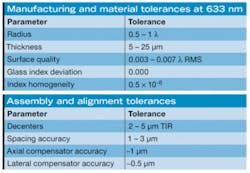
Because of difficult wavefront requirements, fabrication and assembly tolerances of high-NA deep-UV objectives can be very tight. Special assembly and alignment techniques using multiple compensators are required.2 For an rms wavefront error of λ/20, typical tolerances include a thickness of 5 to 25 µm and a glass index deviation of 0.0002 (see table).To achieve tight performance specifications, optical design reoptimization (recomp) is used to correct for parameters that cannot be achieved with very high accuracy, but can be accurately measured during optical fabrication. These parameters include radii, thicknesses, and optical surface errors. Most radius and thickness errors, as well as axially symmetrical surface errors, can be corrected by spacing adjustments. Nonsymmetrical and high-order surface errors can be partially compensated by element rotations about the optical axis (wavefront clocking).
During alignment, the user can compensate for manufacturing errors such as initial assembly errors and material index inhomogeneity, which is uncorrectable at the recomp phase. High-NA objectives are very sensitive to misalignment. In particular, the lack of cement in the deep-UV makes air-spaced doublets and triplets very sensitive because of the high power needed for axial color correction. Even very tight assembly tolerances can induce some high-order wavefront errors across the field. Thus, multiple axial and lateral alignment compensators with different sensitivities to low- and high-order aberrations are needed. Compensation is based on interferometric wavefront measurements. If necessary, the designer can consider field curvature and distortion data in the alignment phase.
Alignment can only compensate for aberrations sensitive to optical element motions. Some wavefront errors, especially high-order deformations induced by optical surfaces and material index inhomogeneity, are not correctable at recomp and alignment phases. Repolishing a preselected and designed-in surface based on objective wavefront characteristics can compensate for these errors. One or more correction surfaces can be involved for combined corrections over the pupil and across the field. To be effective, the designer must optimize these surfaces early on. The spatial frequency and amplitude of the wavefront correction determines the polishing tool size and type. Accuracy of correction is largely defined by metrology. Using these correction surfaces as a final correction after assembly is a key enabling technology in achieving the tight wavefront requirement.
Polarization purity
Ideally the systems engineer would like the objective lens to be as neutral as possible in transferring an image through the system. Pupil filtering and illumination configuration are best done in functionally, if not physically, separate modules. Intensity apodization in the pupil and polarization purity across the pupil are two constraints that the design must address. These are connected in that intensity apodization can be caused by polarization nonuniformity. Both can have large impacts on the final image quality.
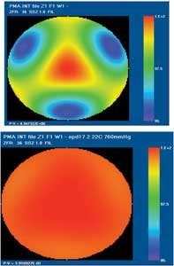
For most applications, the design goal for transmission nonuniformity across the pupil of the objective should be zero. The advantage of a high-NA design can be lost if the image information carried at the edge of the pupil is not transmitted by the objective. Sources of nonuniformity can be optical coatings on the lens element surfaces, bulk absorption in the lens material, nonuniform scatter, stress birefringence, and intrinsic birefringence if a crystalline material like CaF2 is being used. We will briefly look at two sources: antireflection (AR) coatings on the lens elements and intrinsic birefringence of CaF2 lens elements.
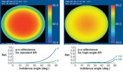
The usual way of describing the transmission properties of the objective is to use the Jones matrix formalism. The field and polarization state of an incoming ray is represented by a vector, the Jones vector, with components referenced to a defined coordinate system. The outgoing ray is likewise represented by a Jones vector. The goal of the designer is to optimize the Jones matrix, which transforms the input vector to the output vector, so that the transformation of the incoming Jones vector results in the desired pupil uniformity and polarization properties. For an AR coating on a surface, this requirement imposes a p-s polarization splitting specification. High-NA objectives may have surface ray angles approaching 60°. Standard AR coating designs may be adequate up to 30° but can exhibit p-s splitting differences of several percent as the angle exceeds 30° (see Fig. 2). Increasing the complexity of the coating design can minimize the transmitted p-s intensity difference through the surface and minimize the linkage of the crossed states.Driven by the need for higher resolution and throughput, mask and wafer inspection systems will continue to challenge designers to juggle many complex design parameters while matching the increased performances roadmap of users. Given the right level of expertise in optical design, fabrication, optomechanical development, and assembly, good designers can meet these challenges.
REFERENCES
1. W. Vollrath, Proc. SPIE 5865, 0E, (2005).
2. T. Sure et al., Optical Fabrication, Testing, and Metrology II, Proc. of SPIE 5965, 1H, (2005).
3. J.H. Burnett et al., J. Microlith., Microfab., Microsyst. 1(3) 213 (Oct. 2002).
STANISLAV SMIRNOV and KIRILL SOBOLEV are system design engineers, BRUCE TIRRI is senior system design engineer, RICK LEWIS is manager of development programs, and ADEL JOOBEUR is senior m anager of optical design and development at ASML Optics, 77 Danbury Rd. , Wilton, CT 06897; e-mail: [email protected]; www.asml.com.


