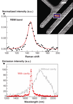
Although emission from direct-bandgap, semiconducting, current-injected carbon nanotubes is weak, spectrally broad, diffuse, and nondirectional in nature, researchers at the IBM Thomas J. Watson Research Center (Yorktown Heights, NY) have streamlined carbon-nanotube emission by integrating a carbon-nanotube emitter with a planar microcavity as a first step toward the development of nanotube-based photonic devices.1
This nano-emitter is essentially a back-gated, light-emitting field-effect transistor (FET) based on a semiconducting single-walled carbon nanotube in a planar λ/2 optical microcavity formed by two mirrors. The microcavity is fabricated with three dielectric layer stacks–250 nm of polymethylmethacrylate (PMMA), 22 nm of aluminum oxide, and 250 nm of silicon oxide–sandwiched between a top gold mirror (20 nm thick) and a bottom silver mirror (100 nm thick). A single nanotube is placed on top of the aluminum oxide layer and is oriented parallel to the top and bottom mirror layers for optimum coupling of the carbon nanotube to the modes of the microcavity. The gold mirror is partially reflecting to allow for out-coupling of the cavity mode.
Because the silicon oxide gating material formed on top of the metal is generally subject to high gate leakage, special deposition steps were performed to ensure smoothness and high quality of the gating layer for reduced leakage and better contact with the nanotube. With the source and gate electrodes of this nanotube-FET grounded and the drain electrode biased at about -10 V, the resulting drain current ranged between 5 and 10 µA.
Narrow spectrum
Raman scattering spectra from a nanotube without the top gold mirror was measured for a carbon nanotube with a diameter of approximately 1.7 nm (see figure). Electrons injected from the drain accumulate kinetic energy in the high-field region near the Schottky barrier and create excitons through impact excitation. Compared to bulk solids, this effect is greatly enhanced in a nanotube and the radiative decay of these excitons causes light emission at approximately 1900 nm without the top gold mirror (free-space emission). Incorporation of the nanotube in the microcavity dramatically modifies the nanotube emission properties. The result is a narrower spectrum with a full-width half-maximum value of approximately 40 nm. The emission spectra from the same nanotube with and without the cavity were measured and compared.
The experiments were repeated using a variety of semiconducting single-walled nanotubes with different dimensions and microcavities with slightly different mirror separations. The result is a spectral narrowing of the free-space emission of the nanotube that matches the spectral position, line shape, and linewidth of the longitudinal mode of the microcavity, regardless of the nanotube dimensions.
The researchers estimate that current-driven nanotubes integrated in silicon nanocavities with a high quality factor and small mode volume could lead to low-threshold on-chip nanolasers, or at least high efficiency on-chip nano-emitters. “The semiconducting carbon nanotube is a truly nanometer-scale material system with excellent optical and electronic properties, says Fengnian Xia, research scientist at IBM Thomas J. Watson Research Center. “Integration of carbon nanotubes with high-confinement photonic devices might lead to different types of active nanoscale photonic devices such as emitters, detectors, and modulators. These nanoscale photonic devices might be useful in on-chip optical interconnects or quantum optics.”
REFERENCE
- F. Xia et al., Nature Nanotechnology online, www.nature.com/doifinder/10.1038/nnano.2008.241 (Aug. 24, 2008).

