Because extreme-ultraviolet (EUV) radiation is so difficult to produce, any scientist or engineer who happens to come up with a good idea using EUV light is soon confronted with the complexity and large size of EUV sources. If such a source could be shrunk in dimensions from the size of a large optical table to that of an end table or even smaller (with the associated reduction in complexity), it is easy to imagine what scientific advances, or practical innovations, might result.
Now, researchers in the Billionth Uncertainty Precision Engineering group at the Korea Advanced Institute of Science and Technology (KAIST; Daejeon, Korea) have created the prototype of such a device.1 While high-harmonic generation is a well-known way of producing EUV light, it is ordinarily done by focusing intense (higher than 1013 W/cm2 at the focal point) femtosecond-laser pulses onto a flowing stream of gas; the high intensity needed to initiate the nonlinear conversion process necessitates large pulse-amplification setups. The KAIST researchers have added a small nanostructured sapphire plate that increases pulse intensity via plasmon field enhancement. In doing so, they found that the required input-pulse intensity dropped by a factor of a hundred, to only 1011 W/cm2 at the focal point—eliminating the need for any pulse amplification at all, thus greatly shrinking the size of the setup.
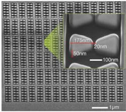
The apparatus includes a modelocked Ti:sapphire oscillator emitting 800 nm pulses of 10 fs duration and 1.3 nJ energy, and a small vacuum chamber containing a lens, the nanostructured sapphire plate, an argon-gas jet flowing over the plate, and a chirped grating along with a photomultiplier tube for spectral measurements. The nanostructure itself consists of a 2-D array of bow-tie shapes (see figure) patterned in a 50-nm-thick layer of gold deposited on the sapphire (a 5 nm layer of chromium was deposited first to aid adhesion of the gold).
The bow ties are each in reality a pair of gold triangles with a small gap between them and are patterned into the gold and chromium using a focused ion beam that produces subnanometer resolution. The ultrafast pulses are incident normal to the plate; as the pulses pass around the bow ties and through the plate, the triangular elements concentrate the pulses’ intensity within the volume in the gap, ionizing the argon gas and creating EUV light. Because the bow ties all act as point emitters, the resulting EUV output is coherent.
The shape of the bow ties was optimized by finite-difference time-domain computer modeling. The values of four parameters—the 175 nm length of the two identical triangular elements of each bow tie, their 30° vertex angle, their 50 nm thickness, and the 20 nm gap between the triangles—were chosen so as to maximize the enhancement of the electric field within the gap.
Modeling and experiment agree
The bow ties and their intensity-enhancement properties were first computer-modeled using Maxwell’s equations, showing an enhancement of greater than 20 dB in the 60 × 50 × 50 nm gap volume, and of 44 dB at the triangles’ two opposing vertices. The experiment then produced EUV radiation, confirming the 20 dB enhancement. The photomultiplier tube (sensitive to radiation of only 200 nm and below) and associated 1 mm slit were moved along the grating’s dispersion line to capture the EUV spectrum, revealing the odd harmonics H7 (113 nm) through H17 (47 nm).
While the tips of the bow ties are greatly rounded in the scanning-electron-microscope (SEM) image, in reality the tips are rounded to from 2 to 4 nm. “The roundness of the tips shown in the SEM image of our paper appears to be a little bit more severe than the actual value of the fabricated tips,” says Sung-Woo Kim, a professor at KAIST. “This is due to the multiple scattering of electrons that occurs around the tip edges in the process of SEM imaging. Furthermore, the imaging resolution of SEM is also limited in the nanometer range.”
Kim, who is also director of a newly founded optical research center within KAIST, notes that he and his colleagues are aiming to boost the EUV-conversion efficiency, and are looking at different shapes and materials for the nanostructures. “We expect that higher harmonics than H17 will be generated by using other noble gases such as krypton, xenon, or mixed gases. In that respect, more experimental work is now under way,” he says.
As for applications, Kim says, “EUV spectroscopy and diffraction microscopy on micro- and nanoscales will be the first practical uses, which we are attempting to demonstrate in the near future.” While another potential use could be as a light source for EUV lithography, a great amount of development would be needed, first to bring the KAIST source’s emitted wavelength from 47 nm down to 13 nm (the standard for EUV lithography), and second, to bring the source’s average output power up from its current tiny level to that of the EUV light source that produced an average 25 W of 13 nm radiation for one and a half hours, which was announced by Cymer (San Diego, CA) in May. However, Cymer’s source will never reach the laptop-computer size possible with the KAIST source—a perfect size for small, portable scientific instruments.
REFERENCE
1. S. Kim, et al., Nature 453, 757 (June 5, 2008).

