The significance of photonics technologies in terms of Europe’s future economic growth cannot be understated. In fact, Europe’s output of photonics products was higher than that of the USA in 2007 and is expected to remain higher in 2008. But what of the future, now that a global economic recession has taken hold? From his unique perspective as general secretary of the European Photonics Industry Consortium (EPIC), Tom Pearsall presents a review of three key photonics market sectors in which Europe leads the world. He discusses the likely effects on these sectors of the current economic climate and the growth outlook for the next year or so.
Tom Pearsall
While growth in Europe’s photonics sector continued through most of last year, the current global economic recession will doubtless affect the industry going forward. Areas that are strongly affected by the downturn, such as automotive manufacturing, will bear the brunt of the recession, while others, like photovoltaics, may weather the storm somewhat better and bounce back sooner.
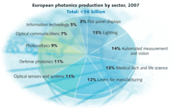
Photonics manufacturing is a high-growth business in Europe. Production in Europe exceeded €54 billion (US$70 billion) in 2007 and is estimated to have reached €61 billion (US$79 billion) in 2008. To put these figures into context, the European production of silicon-based semiconductors was €49 billion (US$63 billion) in 2007, and the value of photonics production in the USA during 2007 was about €50 billion (US$65 billion).
While seven sectors contribute about equally to the overall market in Europe—photovoltaics, defense, optical sensors and systems, production technologies, measurement and computer vision, medical technologies, and lighting—Europe leads the world in the production of photovoltaics, lasers for manufacturing, and lighting (see Fig. 1).
Photovoltaics
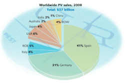
The photovoltaics industry experienced another boom in 2008. Globally, nearly 6 GW of solar/photovoltaic generating capacity was installed, an increase of 67%, raising the total worldwide solar generating capacity to 14.7 GW. Europe was number one for solar/photovoltaic (PV) installations in 2008, representing three-quarters of the worldwide installations. More than 40% of the worldwide installations were made in Spain, which surpassed Germany to take the leading position for solar/PV installations in 2008 (see Fig. 2).
What makes Europe such a popular place? Certainly not the abundance of sunshine! The PV market everywhere is driven by government subsidies in the form of tax credits or feed-in tariff allowances. During the last few years, these have been most generous in Europe, especially Germany and Spain. The leading producers of solar/PV modules are Sharp in Japan and Q-cells in Germany, each of which manufactures about 11% of the worldwide market.
Currently, more than 85% of installed PV systems are based on crystalline or polycrystalline silicon wafers. The performance figure-of-merit for PV is the cost-per-watt of output, and the silicon-wafer approach currently yields the best performance. However, silicon-wafer technology is not sustainable in the long term because there is not enough silicon, nor would there be enough refining capacity to produce silicon-wafer PV cells at the level required for PV to contribute significantly (that is, more than 10%) to the world’s energy supply. Another approach is needed for the future.
Thin-film solar/PV appears to be quite promising. Already the performance in $/watt is similar to that of wafer technology and significant improvements are occurring every year. Improvements in silicon wafer technology, by comparison, are slowing down. In 2008, thin-film technology was used in 15% of installations. There are several thin-film technologies: amorphous silicon, cadmium telluride (CdTe), and copper indium gallium diselenide (CuInGaSe2) are the leading approaches in commercial production. Dye-sensitized solar cells, based on thin films of titanium dioxide (TiO2) nanocrystals, and organic PV thin films are promising technologies in the development stage.1 The thin-film approach also enables deposition on flexible substrates, such as metal or plastic supports. Manufacturing on flexible substrates is a step toward roll-to-roll manufacturing, which has the potential to dramatically reduce fabrication costs and increase manufacturing volumes.
Multijunction solar/PV and concentrated solar/PV are different approaches to reducing the cost-per-watt of output by improving the conversion efficiency. Record performance of 41% power conversion using a multijunction cell was reported by the Fraunhofer Institute for Solar Energy Systems (Freiburg, Germany) in January of this year (the theoretical limit of a silicon-wafer PV cell is less than 27%).
In Germany, most solar/PV installations are undertaken by individuals seeking to benefit from the generous feed-in tariff. These people already have access to the electricity grid, meaning that the purchase is entirely discretionary. Because the installation usually requires taking out a loan, the decision to buy in 2009 may be delayed due to poor economic conditions, uncertainty about employment, and difficulty in obtaining credit. The solar/PV market grew by 60% in Germany in 2007, but only by 40% in 2008. Consumer confidence in the economy will determine the result in Germany in 2009.
In Spain, most solar/PV installations are large “farms” producing 50 to 100 MW of power and installed by international engineering consortia that include the power utilities and local authorities. In 2008, 2.5 GW of generation capacity was installed. In October 2008 the national government decided to reduce the extraordinary growth rate of solar capacity in Spain by limiting the subsidies to cover only 500 MW per year. This decision will reduce the installation of new PV capacity by 80% in 2009.
Solar/PV installations in the USA, which is in fourth place with 1.2 GW of installed power, stand to benefit from a generous and comprehensive tax-credit program that was enacted as part of the TARP rescue plan for the banking industry in October of 2008. As in Germany, consumer confidence and credit availability will play a deciding role in 2009.
Taking these factors into account, we estimate that global installations of PV capacity may reach 3.6 GW in 2009, based on current pricing. This would represent a decline of 38% from the record levels of 2008. Benefiting from a well-established market and a large installed base, Germany will remain in first position for 2009. It is possible that the USA, Spain, and Japan will all show similar levels of installed solar/PV generation capacity by the end of 2009.
Lasers for manufacturing
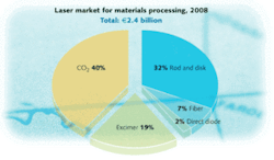
The worldwide market for industrial lasers was €6.5 billion (US$8.45 billion) in 2008, according to Optech Consulting (Tägerwilen, Switzerland). Cutting and welding with lasers has brought a revolution to manufacturing by reducing cost and waste while speeding up processing. Nowhere have the benefits of this innovative technology been felt more than in the automotive industry, a major European industry sector. Various laser technologies are used for materials processing (see Fig. 3). Sales of new lasers in this €2.4 billion (US$3 billion) market segment are currently dominated by CO2 and solid-state systems.
Compared to photovoltaics, the annual growth rate of lasers for manufacturing has been modest (about 5% per year) during the past eight years. However, the emergence of fiber lasers has added a new dynamic to this market. Although fiber-laser sales represent only about 7% of the materials-processing market, their sales have increased at an impressive compound annual rate of 42% since 2005. Fiber lasers are displacing CO2 and diode-pumped solid-state systems in specific materials-processing applications because the higher beam quality enables higher throughput at lower cost. And because of their value proposition these lasers are likely to capture a significant fraction of laser processing applications and markets.2
Intense R&D activity is taking place in Europe to explore and develop the possibilities for fiber-laser technologies in traditional markets, like materials processing, but also for new applications, such as in the medical sector. For example, a four-year European project named Leadership in Fiber Laser Technology (LIFT) will invest €17 million (US$22 million) to develop new higher-brightness fiber-laser sources.
More development work will be needed before fiber lasers can replace current technology in many applications in materials processing, medical therapy, information technology, and defense. Arnold Mayer, of Optech Consulting, emphasizes that materials processing comprises many applications, each of which requires its own set of laser parameters, and not all of which suit current fiber lasers. Materials processing is far from being a homogeneous market.
In thin flat-sheet cutting, which is the biggest single application in materials processing, fiber lasers emitting at 1 µm have several advantages. The pathway to greater market share lies in improving the fiber laser itself, especially solving the problem related to photodarkening of fibers, and the development of improved process technology for cutting thicker materials.
Materials processing by cutting and welding represents more than 50% of the application space for industrial lasers. Revenues in the industrial laser market depend principally on investment by the automotive industry in new manufacturing resources. Microprocessing applications, such as direct laser lithography for manufacturing of flat-panel displays or photovoltaic panels represented an additional 22% of revenues for industrial laser systems in 2008. The significant reductions in automotive production this year will clearly have a major negative impact on industrial laser revenues.
We expect overall industry revenues to decline by 31% from €6.5 billion (US$8.4 billion) to €4.5 billion (US$5.8 billion) in 2009, which is similar to the level of industry revenues in 2003.
Ulrich Hefter, technical director of Rofin-Sinar Laser (Bergkirchen, Germany) comments, “In a growing laser market for materials processing, fiber lasers last year had a market share of about 7% as compared to the year before of 6%; that is, fiber lasers are gaining market share but are still at a low level compared to CO2 and solid-state lasers (72%). I think this is normal for a new technology entering the market.” As fiber lasers become a mainstream manufacturing tool, Hefter foresees a coexistence of different technologies rather than the dominance of a single approach.
About the current business situation, Hefter added, “The machine-tool business, including lasers, has declined by about 50%. This is not only due to the situation in automotive manufacturing and the recovery won’t come only from the automotive business.”
In 2009, fiber lasers should continue to build market share (in a declining overall market) in thin-sheet metal processing where they bring advantages of higher throughput manufacturing at lower cost and a smaller footprint on the factory floor. At EPIC we expect fiber-laser revenues of €180 million (US$233 million) in 2009, representing a 26% decline, compared to 2008. This is a somewhat larger drop than the 15% revenue decline forecast by IPG Photonics (Oxford, MA), the fiber-laser industry leader with a 75% market share.
Lighting
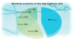
European companies Philips (Eindhoven, The Netherlands) and Osram (Regensburg, Germany) dominate the global lighting market with 42% of the €43.8 billion (US$57 billion) in revenues in 2007. Inside this global lighting market, the composition of the LED lighting segment looks quite different from the overall picture. The leading manufacturer of ultra-high-brightness (UHB) LEDs is Nichia (Tokoshima, Japan) with about 20% market share. After Nichia comes Osram with about 10%. Philips and several other companies follow with 4% to 6% of worldwide sales. Almost half of UHB LEDs are produced by companies in Japan (see Fig. 4).3
About one-fifth of global lighting revenues come from the sale of energy-inefficient incandescent light bulbs, the use of which will be outlawed by 2012 in Europe. Fluorescent fixtures and light bulbs account for 74% of sales, with high-intensity-discharge lamps making up another 15%, and halogen lamps accounting for 8%. The UHB LEDs accounted for 3% of lighting purchases in 2007. The worldwide UHB LED market was €3.4 billion (US$4.4 billion) in 2007, according to Strategies Unlimited (Mountain View, CA), with little additional growth in 2008. Osram and Philips are both leading an aggressive campaign to replace incandescent light bulbs by high-efficiency compact fluorescent lamps (CFLs)—most of which are made in China, leading to strong growth in this market segment.
Although LEDs and CFLS have similar wall-plug efficiencies, there are differences in performance and price. With CFL lighting selling at one-fifth the price of an LED equivalent, it is unlikely that LEDs will be competitive in the consumer lighting market during the next few years. However, the commercial market will benefit from LEDs used with intelligent ICT (information and communication technology) networks that control intensity, color rendition, and light positioning in real time and in response to actual ambient conditions. Thus, the future for LED-based lighting is predicated on the integration of LEDs in luminaires that are designed to exploit the inherent advantages of LEDs in delivering high-quality and intelligent lighting.
Significant economies of energy consumption are possible by developing intelligent LED-based lighting in commercial buildings. Implementation of intelligent lighting will have a direct impact on lowering greenhouse gas emissions and slowing the pace of global warming, which is an important issue in Europe where Germany, Poland, and many countries in Eastern Europe continue to generate most of their electricity by burning coal.
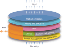
The performance of LEDs can still be improved. According to measurements reported by Michael Kramer of Perkin-Elmer Optoelectronics (Pfaffenhofen, Germany), the wall-plug efficiency of the best UHB LEDs today barely exceeds 25%. Kevin Dowling, VP of Engineering at Philips—Color Kinetics (Burlington, MA), notes that the LED layer, where electrons are converted to photons with nearly 100% efficiency is just one of many important components of a high-performance lighting device. Thermal management is one area where improvements need to be made, with the goal of reducing energy loss through heat generation to less than 25% of the optical output power (see Fig. 5).
The growth of the LED market in outdoor lighting is closely related to the demonstration of energy efficiency. Projects built in 2009 have been planned for several years and funds are already committed. Strong growth in this sector of 25% to 30% in units sold will be maintained at least for 2009. However, ongoing development of LED technology will reduce average selling prices even while performance improves, as described by Haitz’s Law (see en.wikipedia.org/wiki/Haitz’s_Law), so the revenue growth from this segment will be only 5% to 10%.
The automotive business is suffering a serious decline. Toyota, perhaps the world’s most successful automaker, has announced a reduction of 40% in car production in February 2009 compared to February 2008. Declines are steeper for luxury cars where LED lighting is more heavily used. Unlike the architectural lighting market, automakers are responding very quickly to the economic recession, and are unlikely to build up inventories of LED lighting units waiting for a market upturn, particularly in the context of Haitz’s Law. Unit sales are expected to drop 50% for this application in 2009.
Flat-panel displays constitute the single largest segment of the worldwide photonics market with more than $85 billion in sales in 2007. Growth in this market leveled out in 2008, partly influenced by deteriorating economic conditions, but also because the cell-phone industry has not yet introduced a new generation of mobile handsets. Sony-Ericsson, a major player in this sector, has issued a profit warning for 2009 based on a decline of 37% in unit sales for the first quarter of 2009. Analysts predict an industry-wide fall of 15% in unit sales for 2009.
Overall, we expect a 10% decline in unit sales for the UHB LED sector in 2009, which translates to revenues of €2.5 billion ($3.2 billion) , representing a 27% decline in revenues to the level of that of 2004–2005. While this market is global, we expect to see less impact in Europe because there is no manufacturing activity in flat-panel displays, this being almost entirely concentrated in Asia.
Photonics is a global industry, and production of photonic components and systems in Europe is making a strong, balanced, and growing contribution. We have highlighted three areas where that contribution is particularly strong: photovoltaics, lasers for manufacturing, and solid-state lighting. The current worldwide recession will have a negative effect on photonics production in Europe, as everywhere. Some sectors, such as telecommunications, appear to be doing better than others. Other sectors linked strongly to car manufacture, like UHB LEDs and high-power lasers, will be strongly challenged. The photovoltaic market in 2009 will be turbulent because of significant inventories and changes in subsidies. It is too early in the recession to know how consumer confidence will evolve. However, the long-term future for solar/PV remains bright, and strong growth should characterize this sector as soon as we can return to conditions of economic growth and stability.
REFERENCES & RESOURCES
- In 2009, EPIC is organizing a workshop on thin-film and third-generation solar-PV technologies and markets. For more information see www.epic-assoc.com
- In 2008, EPIC hosted an industry workshop in Dresden to examine the potential of fiber lasers. The report from this workshop is available through Optech Consulting (www.optechconsulting.com).
- In 2007, EPIC organized an international workshop in Berlin in 2007 to examine both production and marketing issues for LED lighting. The report from this workshop is available through Yole Développement (www.yole.fr)
Tom Pearsall is General Secretary of EPIC—The European Photonics Industry Consortium, 17 Rue Hamelin, Paris 75016, France; e-mail [email protected]; www.epic-assoc.com.
Tell us what you think about this article. Send an e-mail to [email protected].
