Fiber lasers provide the best combination of focusability, power stability, and efficiency available in the industrial laser market. Of interest to the photovoltaic (PV) industry is the small footprint and high efficiency of these lasers.
Short-pulse fiber lasers are displacing conventional diode-pumped and lamp-pumped solid-state lasers in certain applications. These Q-switched fiber lasers offer cost and operational efficiency but no fundamental difference in pulse performance.
Pulsed fiber lasers using directly modulated seeds have now been introduced that do not rely on Q-switching to generate the pulses. This gives significantly more flexibility in terms of pulse frequency, pulse length, and peak pulse power, giving users a broader range of processing parameters.
This configuration enables peak pulse powers in excess of 14kW to be achieved at 25kHz with an average output power of 20W. The unit also has a high pulsing frequency range from 1 to 500kHz, with pulse widths in the 10–200nm range.
A broader range of pulse parameters can help to refine processing applications. Operating at higher frequencies, specific benefits have been identified for a wide range of materials processing applications. These include marking, thin film patterning, and micromachining applications relevant to photovoltaic manufacture.
One commercially available range of lasers offers an M2 <2, giving beams that have high peak power and small focused spot sizes. However, in some applications the high peak intensity gives rise to undesirable substrate damage. A newly released 30W laser with a higher M2 = 3.2 covers applications where a broader line width or large-area patterning is required and the application benefits from a generally broader power distribution.
These directly modulated MOPA lasers were originally developed as marking lasers, but their enhanced capabilities have led to a range of micromachining processes that go well beyond straightforward marking applications.
Scribing molybdenum films
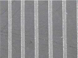
A thin molybdenum (Mo) film on the order of a few microns thick on glass provides an electrically conducting back contact film for CIGS modules. The initial laser scribe requires the selective removal of the molybdenum from the glass substrate. These films are typically 0.25–1µm thick and can be processed at speeds up to 4m/s using laser parameters of 125kHz at an average power of 20W, giving 30µm wide lines. In the sample shown in Figure 1 these are on a pitch of 200µm.
Careful control of the pulse energy is crucial in order to completely remove the film and to produce minimal burr to the patterned edge, lack of cracking/delamination of the Mo film, and no damage to the glass substrate.
Scribing TCO films
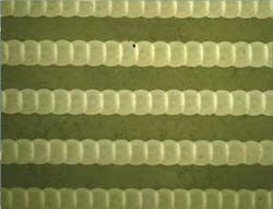
In many thin film modules a transmissive conducting oxide (TCO) film is employed and needs to be patterned in a similar way. The pulse energy required can vary quite significantly. Differing film thicknesses, compositions, and even deposition techniques influence ablation speeds. Films requiring high pulse energy can be processed at low frequencies and speeds of 0.5m/s, but for applications where low energy is required, processing at 5m/s can be achieved at 375–500kHz. A recently introduced addition to the range is a higher average power 30W laser. This pushes the maximum pulse energy up to 1mJ. The higher M2 of 4 enables larger spots for marking many materials faster and has an additional benefit of producing a flatter top beam. This improves the quality of scribes (see Figure 2).Edge deletion scribes
The removal of all three of the films from a 12mm-wide band around the edge of amorphous silicon thin film cells requires high peak power, good pulse energy control, and stability. The higher mode of the 30W laser means that low levels of overlap are required, giving good coverage rates. With 30W, 2cm2/s removal can readily be achieved. Machines using multiple lasers to achieve the desired volume removal rates enable greater flexibility to the end user and can be lower cost than a single high-power laser source.
Silicon nitride ablation
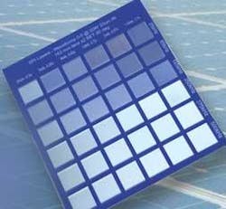
Due to the high absorption of silicon nitride in the IR, a high repetition rate, low pulse energy combination produces clean, high speed removal (see Figure 3). Removal at rates of >1cm2/s can be achieved using a repetition rate of 375kHz, 20W from either glass or silicon substrates. Optical examination has shown that a smooth surface with efficient removal of the silicon nitride is achieved at a threshold value of 250kHz. This is probably due to the enhanced interaction time related to high repetition rates.Silicon processes
Silicon is widely used in the photovoltaic industry both as single and polycrystalline forms and as thin films. There is now evidence to suggest that the room temperature absorption depth of a near IR beam in silicon of 0.2–0.3mm is misleading. At higher temperatures, such as those achieved on a very short timescale during high power density laser ablation, this absorption depth drops dramatically. Also, the less pure forms of silicon used in the solar industry absorb solar radiation across the complete solar spectrum and hence absorb better in the near IR. Combining this with the new duty cycle parameters opened by these fiber lasers brings new applications within the capabilities of these directly modulated nanosecond fiber lasers.
These applications include simple scribe and break, drilling, and edge deletion in solar cells. The key feature requirements of these applications are narrow lines, low HAZ, minimal surface debris, and no burr. Low frequency, high pulse energy can generate deep scribes but suffer high levels of HAZ and debris. Once again, using higher frequencies and lower pulse energies enables much finer control of the heat input.Marking
These lasers are now well established as conventional marking lasers for marking both plastics and metals. In many cases, the additional high repetition rate capability adds further process flexibility and a completely new level of process control or fine tuning of processes. An example of this is during deep laser engraving, a high speed, high repetition rate smoothing pass can be used to 'polish' the base of an engraved mark, enhancing contrast and readability. Solar glass is typically transparent to IR, but with the use of special tapes, permanent, crack-free, 2D data matrix marks on glass have been developed. Optimal results are achieved at high repetition rates of >250kHz.
Conclusions
A novel type of directly modulated fiber laser has been introduced with unique capabilities offering process advantages for numerous solar applications. The advantages of high repetition rates have now been proven industrially and are helping to reduce the cost of solar cell manufacture. The versatility of operation over a wide range of pulse frequency, pulse energy, peak pulse power, and pulse duration gives very fine process control and operational flexibility.
