SANJAY KRISHNA
As infrared focal-plane arrays (FPAs) have evolved from the first generation of linear arrays to the second generation of small-format staring arrays to the current “third-gen” devices, there is an increased emphasis on large-area focal-plane arrays with multicolor operation and higher operating temperature. To achieve these characteristics, increased functionality at the pixel level needs to be developed. This functionality can manifest itself as spectral, polarization, phase, or dynamic-range signatures that are able to extract more information from a given scene.
History of IR imaging
The midwave IR (MWIR; 3–5 µm) and long-wave IR (LWIR; 8–12 µm) portions of the electromagnetic spectrum are technologically important for three main reasons. The first is that most objects emit radiation in this wavelength range; thus, IR sensors are effective at “seeing in the dark” and are useful for applications such as night-vision imaging, thermography for noninvasive medical imaging, and civilian diagnostics. The second reason is that most chemical species have spectral signatures in the IR regime due to fundamental absorption processes associated with vibrational states of the molecules, making IR sensors important for applications such as pollution monitoring and gas-leak detection. And finally, the atmosphere has clear transmission windows in the MWIR and LWIR, making these bands attractive for terrestrial imaging applications.
High-performance cooled MWIR and LWIR detectors provide the best performance, albeit at a high cost.1 Detectors in this market are currently dominated by bulk indium antimonide in the MWIR and mercury cadmium telluride (MCT) in the LWIR. Both these semiconductors have bandgaps in the appropriate bands; incident photons that are above the bandgap create photogenerated carriers (electrons in the conduction band and holes in the valence band), usually in a biased p-n junction.
Another class of detectors with promise for the LWIR regime is intersubband devices based on transitions in quantum wells; these are referred to as quantum-well IR photodetectors (QWIPs). Most QWIPs are operated in a photoconductive mode, in which an external bias is applied to tilt the energy bands to collect carriers that are generated when incident photons are absorbed due to the resonance in the intersubband states. However, QWIPs have been plagued with problems associated with large dark current and low quantum efficiency, primarily arising from the nature of the intersubband transition.
There is also active interest in investigating IR detectors based on intersubband transitions in quantum dots. These detectors, called quantum-dot IR detectors (QDIPs), are expected to have a lower dark current due to their three-dimensional confinement and increased lifetime as a result of reduced scattering processes. More recently, quantum-dots-in-a-well (DWELL) detectors have been proposed. These detectors combine the advantages of QWIPs, such as control over the operating wavelength, with the advantages of QDIPs, such as normal-incidence operation, increased lifetime, and three-dimensional confinement. Lately, a very promising technology based on miniband transitions in Type II strained-layer superlattices of III-V materials has emerged that offers high quantum efficiency.
First- and second-generation IR detectors, which were dominated by single-pixel, linear, and staring small formats (1000 to 100,000 pixels), were developed from the 1950s to the 1990s. In the past decade, the emphasis of the R&D community has been on developing the third-generation systems, which are large-format (1 to 16 megapixels), have higher operating temperature (200 K to 250 K for MWIR, and 120 K to 150 K for LWIR), and achieve multicolor operation. However, most of the today’s MWIR/LWIR FPAs are “black and white” detectors and only monitor the emissivity in a given scene without extracting any spectral information. Thus, if an object appears dark in the image, one does not know whether it is due to low emissivity or low temperature of the object.
Infrared retina
We believe that the emphasis for the next-generation device will be on incorporating enhanced functionality in the imagers, preferably at the pixel level. The basic idea is to pack as much information as possible into the pixel itself, resulting in an “infrared retina.” Thus, the individual pixels in the focal-plane array, which would act like the cones in the human eye, would not only monitor the emissivity of a given scene but also record the spectral features in the scene. One could also envision that the individual pixels could be made polarization-sensitive or have a wide dynamic range through the incorporation of gain in the pixel. These signatures would be coupled with powerful on-chip signal-processing algorithms to extract information from the scene, which would lead to a dramatic reduction in the size, complexity, and cost of IR-imaging systems.
For example, traditional multispectral or hyperspectral IR sensors either use multiple arrays, each of which responds to a different wavelength band, or use a series of external filters to spectrally limit the incoming radiation. However, the use of multiple arrays and the complexity of the spectral calibration of an individual array increases the cost and limits the performance of these sensors. If one can demonstrate spectrally tunable and wavelength-agile MWIR/LWIR sensors in which the detection mode is collocated and simultaneous, such sensors would provide access to a totally new set of data not now available from conventional sensors.
There are a number of approaches that may provide this enhanced functionality that will form the basis of an infrared retina. The following list is not comprehensive, as there are several other approaches that have also been proposed and are being actively pursued.
Photonic-crystal cavities
One approach to improving the spectral resolution of IR detectors is the use of a resonant cavity to limit the absorbed spectrum and increase the responsivity of the detector. But the thickness of the reflecting layers becomes extremely large (a periodic spacing of around 3 µm for each Bragg stack for a 10 µm wavelength), making this approach unfeasible for large-scale manufacturing.
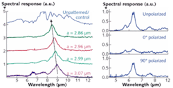
We have been exploring the possibility of defining a plasmon-assisted photonic-crystal (PC) cavity for each multispectral/hyperspectral pixel. The finesse, or Q factor, of the PC cavity can be made as high as 105 in state-of-the-art PC designs. A high Q will ensure that there is an “amplified” spectral response, leading to an increase in the responsivity and sensitivity of the detector and an associated narrowing of the spectral response. Preliminary results from this technology (in collaboration with researchers at Caltech) have led to an enhanced conversion efficiency, spectral tuning, and polarization control (see Fig. 1).2
Voltage-tunable spectrally adaptive sensors
We have also been able to realize spectrally adaptive sensors that are bias-tunable by exploiting the quantum-confined Stark effect in the DWELL heterostructure.3 The quantum-confined Stark effect can be combined with a projection algorithm to produce a continuously tunable detector with overlapping bands that can be used for target recognition.
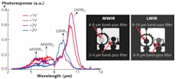
An intermediate approach is to exploit the multiple transitions present in the DWELL structures to obtain collocated two-color detectors using the same active region. The DWELL spectral response can be exploited to obtain two-color detection within the same wavelength band (MW/MW or LW/LW) or detection in two different bands (MW/LW; see Fig. 2).Information in the two colors can either be obtained in a sequential fashion in subsequent frame cycles or in a quasi-simultaneous scheme in which the two bands are obtained in subframe cycles. For such a detector, one would require a high-end digital-readout integrated circuit (ROIC) to provide this wide bias range. Several companies are developing low-noise digital ROICs with such bias functionality; for example, Raytheon Vision Systems (Goleta, CA) has recently reported a two color MCT detector with a MWIR and LWIR diode in a back-to-back configuration with a floating p region.4 Such an ROIC can be integrated with the detector to provide this enhanced functionality using a simple “single-bump” per pixel design.
Enhanced gain using an avalanche photodiode
Another proposed approach involves incorporating gain in the detector. One embodiment of such a device, called a quantum-dot avalanche photodiode (QDAP), is expected to demonstrate improved performance over conventional quantum-dot detectors.5 In the QDAP, an intersubband quantum-dot detector is coupled with an avalanche photodiode (APD) through a tunnel barrier. The tunnel barrier reduces the dark current while the APD provides the necessary photocurrent gain to increase the signal-to-noise ratio. In particular, the APD is expected to provide the gain necessary to overcome the readout noise (including 1/f and preamplification Johnson noise) and achieve a significantly enhanced signal, which comes at the slight expense of the avalanche excess noise.
With this novel combination, one can achieve a higher sensitivity at the same temperature (D*a responsivity) or have a comparable performance at higher operational temperatures. This is very exciting, as it also opens up the possibility of obtaining Geiger-mode and single-photon operation in the MWIR/LWIR, which has not been demonstrated before.
Acknowledgments
The author would like to acknowledge all his research group members, including Prof. Dawson, Prof. Stintz, Drs. Plis and Sharma, and graduate students Rajeev Shenoi, Stephen Myers, John Montoya, David Ramirez, Jiayi Shao, Hasul Kim, Eric Jang, Arezou Khoshakhlagh, Nina Wiesse Bernstein, Ajit Barve, Jonathan Andrews, and Nutan Gautam. Support from funding agencies (NSF, AFOSR, AFRL, ARL, MDA, DARPA, IC Postdoc and KRISS-GRL) is also acknowledged.
References
- A. Rogalski, Infrared Photon Detectors, SPIE Press, ISBN 978-0819417985 (1995).
- Posani et al., Appl. Phys. Lett. 88(15) p.151104 (March 2006).
- S. Krishna et al., U.S. Patent 7,217,951 (2007).
- E.P.G. Smith et al., J. Electronic Materials, June 2006.
- S. Krishna et al., U.S. Patent 7,271,405 (2007).
Sanjay Krishna is an associate professor of electrical and computer engineering at the Center for High Technology Materials at the University of New Mexico, 1313 Goddard SE, Albuquerque NM 87106; e-mail: [email protected]; www.chtm.unm.edu.

