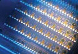
Monolithically grown germanium/silicon APDs have high sensitivity, low noise, and world-record gain-bandwidth product. They are also CMOS-compatible and can be used at common optical-communications wavelengths.
YIMIN KANG and MIKE MORSE
Since avalanche photodetectors (APDs) were developed more than half a century ago, device engineers have worked to improve their performance and expand their applications into diverse new areas wherever high detection sensitivity is needed. Low noise, high gain, and large bandwidth are always desirable features for APDs, especially when they are being used as an alternative to p-i-n-type photodetectors in optical-communications. As a result, most APD research has been focused on lowering the avalanche excess noise and improving gain-bandwidth product (GBW) through material and structure optimization.1
III-V devices
In long-distance fiber-optic networks, optoelectronic devices are dominated by those made from III-V semiconductor compounds due to the ability to easily tailor the strain and bandgap of the device. Through decades of development, III-V-based APDs have evolved from a p-i-n structure to a separate-absorption-and-multiplication (SAM) structure and a few derivatives thereof. In the resulting devices we see today, light absorption and carrier multiplication take place in separated regions/materials. As a result, the dark current and excess noise of an APD can be optimized independently.
null
To further reduce the excess noise, another option is to choose a multiplication material that has asymmetric carrier impact ionizations when the avalanche breakdown happens, such that only one type of carrier predominates the avalanche process. This material property is qantified by the ratio, k, between the ionization coefficient of electron, α and hole, β. A lower k value also results in higher GBW. Therefore, the traditional multiplication material—indium phosphide (InP), with a k of around 0.4 to 0.5—was replaced by indium aluminum arsenide (InAlAs), with a k in the region of 0.2 to 0.4. InAlAs serves well at data rates up to 10 Gbit/s, but with the disadvantages of requiring a sophisticated layer structure and complicated processes. When the data rate increrases to 40 Gbit/s, as is happening now, the resulting limited GBW reduces the APD receiver sensitivity improvement to only a couple of dB over p-i-n-based receivers.
On the other hand, bulk silicon (Si) offers excellent noise characteristics (k as low as 0.02 to 0.1), which makes it a desirable material for multiplication. In addition, the possibility of implementing CMOS technology and monolithic integration with high-performance Si circuitry is attractive to anyone who wants to bring the traditional optoelectronic systems to a higher level. What makes the use of Si challenging is finding a light-absorption material that is suitable for the telecommunications wavelength window and can be seamlessly integrated with Si. In one recent approach, wafer-bonded InGaAs-on-Si APDs demonstrated a GBW of 315 GHz and k as low as 0.02.2 While promising, issues with this approach arose regarding the bonding interface quality and incorporating III-V materials into CMOS fabrication.
Another material, germanium (Ge), is more promising. It has a bandgap as narrow as 0.66 eV, which makes it suitable for light detection up to about 1600 nm. The replacement of InGaAs with Ge allows the creation of an APD via traditional epitaxial growth despite the 4% lattice mismatch between Ge and Si. Furthermore, Ge has been used inside CMOS facilities for a few transistor generations as a means to improve performance, so there should be no significant barrier to manufacturing Ge/Si devices.
The Ge/Si avalanche photodiode
A normal incidence mesa-type Ge/Si APD consists of three circular mesas: a Ge mesa on the top for light absorption, a slightly larger Si mesa in which carrier multiplication takes place, and a much wider silicon contact mesa sitting on the substrate to minimize parasitic effects (see Fig. 1). The layer structure is specially designed so that at the operational bias voltage, a large amount of electric field builds up inside the Si region while the field inside the Ge remains low—just high enough to fully deplete the absorption layer.
Careful fabrication processes, including epitaxial growth, keep the primary dark current of the diode low—less than 20 mA/cm2 at a gain of 1, which is comparable to or even smaller than that for most of the reported Ge/Si p-i-n photodiodes. However, such a dark-current level is still orders of magnitude higher than that for III-V APDs. This relatively high level is caused by the fact that Ge inherently generates higher dark current than InGaAs, and also by the presence of the underlying dislocations/defects at the Ge-Si interface. Much more work in process improvement needs to be done to overcome this issue.
Photoresponsivity
Typically, the photoresponsivity of an SAM APD with an antireflection coating (ARC) properly applied on the illumination window is primarily determined by the depleted absorber thickness and its absorption coefficient at the wavelength of interest. However, a couple of factors should be to be taken into account while estimating the responsivity of a Ge/Si APD.
First, to reduce an initially high density of dislocations at the Ge-Si interface and inside the bulk Ge, a high-temperature annealing step is usually performed. The side effect of such treatment is to introduce Ge-Si interdiffusion at the interface, which reduces absorption efficiency. The second factor is more positive: the tensile strain in the Ge film has been proved to contribute to the absorption enhancement at long wavelengths. Both factors must be considered while designing the fabrication processes, especially for APDs to be used at long wavelengths such as 1550 nm.
For a Ge/Si APD with a 1-µm-thick intrinsic Ge layer and an ARC, the photoresponsivity is measured to be 0.55 A/W at 1310 nm and 0.18 A/W at 1550 nm. However, when the annealing temperature is lower than 800°C, the Ge-Si interdiffusion impact on the responsivity is negligible. There is room in the Ge/Si APD to further improve the responsivity for data rates up to 10 Gbit/s.
GBW
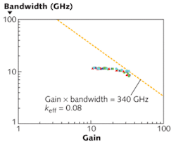
The electrical 3 dB bandwidth of a 30-µm-diameter Ge/Si APD was tested at a 1300 nm. The device’s multiplication gain (the ratio of the responsivity at a given bias voltage to the primary responsivity) was calculated, and the bandwidth with respect to APD gain measured (see Fig. 2). The measured Ge/Si devices exhibit typical APD frequency-response characteristics. The bandwidth remains high at low gain and rolls off beyond a certain gain when the avalanche-buildup time kicks in. For the 30-µm-diameter Ge/Si APDs, the bandwidth is 11.5 GHz for gains up to 20 and the highest GBW obtained is 340 GHz. Such significant improvement in GBW enables a Ge/Si APD to be operated at a gain of 30 to 40, which is triple the gain of a typical III-V-based APD.
As the reverse-bias voltage across the 30 µm Ge/Si APD is increased, the multiplication gain eventually decreases due to the carrier-screening effect. However, the 3 dB bandwidth counterintuitively increases even beyond the highest bandwidth obtained at low gain. The resulting GBW can be several times higher than the traditional avalanche-buildup-time-limited GBW. The highest measured GBW is 860 GHz at -30 dBm optical illumination power, corresponding to a gain of 65.3 and a BW of 13.3 GHz.3 Preliminary simulation and modeling show that the enhanced bandwidth and GBW can be attributed to the inductive component invoked by the delay between the avalanche current and the electric field. A more-detailed analysis of this intriguing phenomenon is under way.
Sensitivity
Sensitivity (the minimum optical signal power that a receiver can detect while maintaining a certain bit-error rate) is the ultimate performance test for optical receivers. It takes various device parameters into account such as photoresponsivity, dark current, excess noise, noise current of the transimpedance amplifier (TIA), bandwidths of the photodiode and TIA, and so on. The sensitivity of the Ge/Si APD was carefully evaluated with receivers in which 30 µm-diameter APDs were wire-bonded with TIAs. At a bit-error rate of 1 × 10-12 and a data rate of 10 Gbit/s, the measured resistivity was -28 dBm at 1310 nm. This result is comparable to the best commercial InP-based APD receivers and only about 1 dB short of the best InAlAs-based APD receivers.
Now that the concept of a monolithic Ge/Si APD has been proved and record-high GBW performance has been demonstrated, future research is aimed at developing waveguide Ge/Si APDs operating at a data rate of 40 Gbit/s or beyond. If the dark current could be reduced through device structure and process improvements, we could soon see Ge/Si APDs starting to replace III-V based APDs in the market.
ACKNOWLEDGMENT
This work is supported by DARPA under contract number HR0011-06-3-0009, and is supervised by Jag Shah in the MTO office. The authors would like to thank Professor Joe Campbell and Professor John Bowers for their contribution to this research.
REFERENCES
- J. C. Campbell, J. Lightwave Technology 25, 109 (2007).
- A.R. Hawkins et al., Appl. Phys. Lett. 70, 303 (1997).
- W. S. Zaoui et al., Optics Express 17, 12641 (2009).
Yimin Kang is a senior optical researcher and Mike Morse is a principal engineer at Intel Corporation, 2200 Mission College Blvd., Santa Clara, CA 95054; www.intel.com; e-mail: [email protected].
Tell us what you think about this article. Send an e-mail to [email protected].


