Planar nanophotonic devices such as waveguides or plasmonic structures often suffer from high insertion loss and, in the case of fiber-optic networks, require complex coupling of the physical planar structure to a cylindrical optical fiber. But what if the nanophotonic device could be physically integrated within the optical fiber structure itself? Just such a capability has been demonstrated by scientists at Friedrich-Schiller-University (Jena, Germany) and at the Max Planck Institute for the Science of Light (Erlangen, Germany); namely, cylindrical nanophotonic structures are embedded directly in photonic crystal fibers (PCFs) or microstructured optical fibers and/or capillary tubes through a pressure-assisted melt-filling (PAMF) process.1
Using PAMF, the researchers are developing PCFs with new functionality, including fabrication of a plasmonic nanoprobe useful for near-field microscopy applications.
PAMF capabilities
After first ensuring that the melting temperature of the material to be infiltrated in the silica fiber or capillary is less than the softening temperature of silica (1400°C), the molten material is pressed into the holes of the fibers under high pressure. Since liquid metals are anti-wetting materials, pressures on the order of several hundreds of bars are needed to fill holes with nanoscale diameters.
Unlike traditional drawing or extrusion techniques, both metal and low-melting compound glasses or even semiconductor materials can be incorporated, while problems with thermal mismatch of materials for small “hole” diameters during the drawing process are avoided.
Examples of unique optical fibers possible with PAMF include capillary filling of arsenic trisulfide glasses in a 1 μm bore diameter, resulting in development of a chalcogenide-silica waveguide that, when exposed to 2 μm wavelength ultrashort pulses, generates a coherent mid-infrared supercontinuum output that extends to 4 μm.
Plasmonic probes, for example
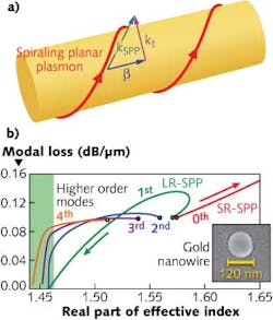
Another novel optical fiber consists of an array of 100 gold nanowires fabricated within a microstructured fiber using the PAMF process. Here, the silica does not interact with the gold material during filling, enabling the implementation of high-quality longitudinal nanowire structures that allow the propagation of plasmonic modes along the thin cylindrical nanowires within the fiber (see figure). These cylindrical plasmonic modes can couple to the mode of the optical fiber into which they are embedded, creating a new class of nanophotonic device.
Using this fiber with its embedded nanowires, the researchers were able to observe superplasmonic mode formation. In addition, using a tip calibration technique, they measured the orientation of a local electric-field vector (nanoscale polarization) with a lateral resolution of better than 60 nm—the first measurement of the transverse near-field pattern of a propagating plasmon mode.
When the end of a tapered nanowire-enhanced fiber is cleaved, metal “cones” with diameters as small as 10 nm are formed. Incoming light excites particular plasmonic resonances at the fiber’s tip end, allowing the fiber to act as a resonant subwavelength probe. “This might lead to a new kind of fiber-based nanoprobe that could find application in biophotonics for DNA sequencing,” says Friedrich-Schiller-University professor Markus A. Schmidt. “Nanowire-based fiber plasmonics represent a new and promising route for accessing new areas that only optical fibers can reach.”
REFERENCE
1. M. A. Schmidt, Nanotech., July 14, 2014; doi:10.1117/2.1201406.005493.

