The combined efforts of members of PLATON—the European Union 7th Framework Programme Collaborative Project, funded since January 2010, that aims to put “plasmonics ‘in-the-box’” and make plasmonic interconnects real through a marriage of plasmonics and silicon photonics—are already bearing fruit. Active plasmonics have been demonstrated in a wavelength-division-multiplexed (WDM) data switching application via a dielectric-loaded surface-plasmon-polariton (DLSPP) thermo-optic (TO) switch developed by PLATON consortium researchers at Aristotle University of Thessaloniki and the Center for Research and Technology Hellas (both in Thessaloniki, Greece), the National Technical University of Athens (Athens, Greece), the University of Burgundy (Dijon, France), the University of Southern Denmark (Odense, Denmark), AMO GmbH (Aachen, Germany), and Fraunhofer IZM (Berlin, Germany).1
The researchers say this is the smallest TO DLSPP-based Mach-Zehnder interferometric (MZI) switch reported so far, and performs successfully in 4 × 10 Gbit/s WDM switching applications with the ultralow power-consumption and high response-time parameters needed for integrated photonics in next-generation high-performance computing and data center applications.
Chip-scale plasmonics
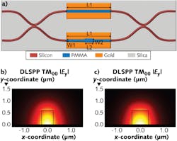
The DLSPP-based MZI switch has active arms comprising 60-μm-long dielectric ridge waveguides of polymethylmethacrylate (PMMA) with 500 nm ridge width and 600 nm ridge height on top of gold stripes that support SPP modes at telecom wavelengths (1550 nm) and effect switching through refractive-index changes in the waveguides as the gold strips are heated.
To avoid the π phase shift and excessive propagation losses that would come with a symmetric MZI configuration, one of the arms of the MZI is modified by increasing the ridge width from 500 to 700 nm in a 6-μm-long section at the middle of the arm (see figure). In this way, a default phase asymmetry of π/2 between the two MZI arms is introduced due to the higher refractive-index value experienced by the DLSPP waveguide mode in the wider PMMA ridge.
On/off switching operation was tested in both static and dynamic conditions by exploiting the TO effect when a MZI arm was electrically controlled. In a single-channel experiment using the output of a 1542 nm laser modulated into a 10 Gbit/s non-return-to-zero (NRZ) data signal and amplified by an erbium-doped fiber amplifier (EDFA) to reach 30 dBm output power, the signal was transmitted through the silicon waveguides and plasmonic arms of the MZI and routed to the MZI’s switched port, experiencing 11 dB total power losses. This switching functionality required 13.1 mW with 3.8 μs switching time and 14 dB extinction ratio (ER) at 40 mA injected electric current.
In a demonstration of WDM switching performance, four optical beams originating from different laser sources (1545.1, 1546.7, 1547.7, and 1549.1 nm) were modulated and multiplexed to a 4 × 10 Gbit/s NRZ data signal that was amplified to 31 dBm total power and subsequently imported to the electrically controlled DLSPP-based MZI. In dynamic control conditions using electrical pulses of 40 mA peak value and 20 KHz repetition rate, successful data switching was realized by the interferometric device, yielding an ER value close to 14 dB for each data channel. Moreover, error-free performance was attained for all channels, both for the MZI’s switched port during the “high-voltage” state and its unswitched port during the “low-voltage” state, implying successful switching operation with bit-error-rate values on the order of 10-9.
“Plasmonics is introduced for the first time in WDM switching applications,” says Nikos Pleros, professor at Aristotle University of Thessaloniki and PLATON project coordinator. “Combined with their small footprint, these devices pave the way for a new ‘beyond silicon photonics’ era in integrated photonics, where circuit designers can choose at will the best solution for IC performance optimization between electrical and optical signals. Continuing progress in plasmonic technology may lead to the necessary broadband, ultrasmall, and low-energy network-on-chip solutions required by computing environments.”
REFERENCE
1. S. Papaioannou et al., Nat. Sci. Rep. (online), 2, 652, 1–9 (Sept. 12, 2012).

