According to the Rayleigh criterion, diffraction effects limit optical-lithography feature sizes to half the wavelength (λ/2) of the light used (semiconductor chipmakers who use optical lithography to create chip features smaller than λ/2 rely on multiple exposures and other specialized techniques). However, researchers continue to find ways to perform subwavelength lithography (without resorting to chipmakers’ tricks) to obtain even smaller feature sizes using unconventional nanolithography and immersion lithography techniques.
Many attempts have been made to advance this field beyond the current limit set by the wavelength of the laser used. These methods are usually based on multiphoton processes, multiple beams, and/or quantum entanglement, making the implementation of these schemes extremely difficult. But a new technique from Texas A&M University (TAMU; College Station, TX) and The National Center of Mathematics & Physics (KACST; Riyadh, Saudi Arabia) that uses two lasers and exploits molecular oscillations in the lithographic photoresist material is simple to implement and achieves arbitrarily small feature sizes.1
Rabi oscillations
When light is incident on an atom or molecule, the electrons within undergo oscillations between the ground state and an excited state. These oscillations are called Rabi oscillations, and their frequency is directly proportional to the intensity of the incident light. In the method proposed by the TAMU-KACST team, a laser at one frequency that is resonant with the energy difference between the ground and an excited state of the atoms within the photoresist material is launched into the photoresist to induce Rabi oscillations. Next, a second laser with a different frequency dissociates the molecules in the excited state, but does not affect those in the ground state. The effect on the dissociated molecules is a change in their chemical properties, especially their solubility. The resulting photoresist patterns are then dependent on the spatial distribution of the excited state induced by the first laser pulse.
The Rabi oscillations induced in the photoresist (by a standing wave created by a laser beam) modulate the number of atoms in the excited state, resulting in a subwavelength spatial pattern in the photoresist with a resolution on the order of the wavelength divided by the number of Rabi cycles. By increasing the intensity of the incident field, the number of Rabi oscillations can be increased, thereby increasing the resolution of the lithographic pattern.
Implementation
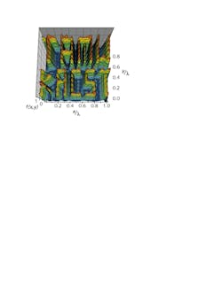
To use the Rabi oscillation model in an actual physical lithography setup, the researchers have explored some possible photoresist materials and laser parameters (see figure). For 1-bromonaphthalene, for example, with a 5 ps decoherence time and laser peak power values of 2.17 GW/cm2 for the beam responsible for Rabi oscillations and 0.13 MW/cm2 for the dissociation laser, feature sizes on the order of λ/10 are possible for a region with dimensions around 10λ. Creating larger patterns in, say, a 1000λ-sized region is possible at those same laser powers using a phase mask and a mask containing 10λ holes.
“Our method for sub-wavelength lithography is only a single preparation step away from the currently implemented lithographic process,” says M. Suhail Zubairy, professor of physics at Texas A&M University. “The beauty of this method is that it is possible to generate nanoscale patterns, and at present efforts are underway at TAMU to implement this scheme in NV [nitrogen vacancy] diamond structures.”
REFERENCE
1. M. Suhail Zubairy, FiO 2011, paper FTuM1 (October 2011).

