SHORTWAVE SEMICONDUCTOR LASERS: Lattice constant is key to group III-nitride-based UV light emitters
ELIAS TOWE and TARUN K. SHARMA
Efforts to harness the benefits of UV radiation have been given a boost as a result of rapid progress in the synthesis of group III-nitride materials. The nitride materials are wide-bandgap semiconductors that can be used to fabricate light-emitting devices in the UV region of the electromagnetic spectrum. They can also be used for light detection in the same spectral band. The majority of efforts are focused on the fabrication of UV light emitters: both lasers and LEDs. The most important and interesting applications of the light emitters include disinfection and sterilization of surfaces and utensils, water disinfection and decontamination, UV curing processes in industry, phototherapy, and medical diagnostics.
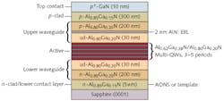
Of the group III-nitride alloy semiconductor family, the aluminum gallium nitride AlGaN alloys are the most versatile for design and fabrication of emitters that span the UV spectrum from the UV-A (400–320 nm) through the UV-B (320–280 nm) to the UV-C (280–200 nm). Most devices reported in the literature have been grown on sapphire substrates. Before the active region is grown, one typically deposits an AlN buffer layer on top of the sapphire substrate as a lattice constant bridge that mediates between the sapphire and subsequent AlGaN layers. This is then followed by a silicon-doped AlyGa1-yN cladding layer on top of which is grown the active region, composed of AlxG1-xN/AlyGa1-yN (y
Before the top contact layer is grown, one of two alternative schemes is generally used to block the escape of electrons from the active region. The first incorporates a high-aluminum-content AlzGa1-zN quantum barrier (z≥0.9). This barrier is followed by a heavily doped p-type GaN contact layer. In a second form of the electron-blocking scheme, other researchers have used a multi-quantum-barrier structure in place of the single quantum barrier. In the latter case, the implementation employs several periods of an AlxGa1-xN/Alz Ga1-zN structure that has been reported to yield slightly better operating characteristics.1
Obstacles to raising EQE
Although some progress has been made in the development of UV light sources, the major obstacle remains the extremely low external quantum efficiency (EQE) of the nitride emitters; there is a notable drop in efficiency as emission wavelengths approach deep-UV.2 The EQE for LEDs is defined as the product of the internal quantum efficiency, carrier injection efficiency, and light-extraction efficiency. The internal quantum efficiency is related to the crystalline quality of the epitaxial layers; fewer defects and dislocations lead to better performance.
If the device structures are grown on sapphire substrates, the lattice-mismatch-induced defects and dislocations (approaching 1010 cm-2 in some cases) cannot be reduced to a desired level on the order of 104 cm-2 or lower. Two other issues that affect mainly the carrier-injection efficiency are a difficulty in achieving highly doped p-type AlGaN cladding and barrier layers, and reduced magnitude of the band discontinuities at key heterojunction interfaces. Also, UV light is absorbed at the p-side electrode.
To minimize the impact of lattice-mismatch-induced defects and dislocations, bulk AlN material has recently been proposed and used as a substrate for UV light emitters.3 The AlN substrate leads to lower lattice and thermal mismatches between it and subsequent AlGaN layers. To reduce dislocations when bulk AlN is used as the substrate, the AlGaN layers grown on top must be sufficiently thin if the Al composition in them is high to guarantee that the structure is pseudomorphic (that is, they maintain the crystalline structure of the substrate). This may represent an unacceptable device design compromise. Although improved performance characteristics in UV LEDs that use this approach has been reported, the EQE for deep-UV LEDs (<350 nm emission wavelength) remains low (<2%).
Residual strain
In a recent paper, we argued that in addition to all the known problems that prevent the fabrication of highly efficient UV emitters, another limitation is the amount of residual strain in the device structures.4 Residual strain modifies the valence-band structure of AlGaN layers used in UV devices in a way that can negatively affect the emitted light polarization properties.5 To complicate matters, UV light emitted from an active AlxG1-xN/AlyGa1-yN multi-quantum-well structure can switch its polarization from transverse electric (TE) to transverse magnetic (TM), depending on the amount of residual strain present in the active layer—which further depends on the choice of template/substrate. When the emitted light is TM-polarized, it is difficult to extract along the c-axis (the direction along which the layers are grown). This leads to decreased light-extraction efficiency, and thus lower overall EQE. Thus, it is important to know in advance the aluminum composition of an AlxGa1-xN/AlyGa1-yN quantum-well structure and its relationship to either the bulk AlN substrate used or the AlzGa1-zN (x
The ideal situation is where the Al content (and residual strain) does not lead to emitted light with a polarization that makes light extraction difficult. This basically implies that once the operating wavelength for a UV emitter has been selected, the active region and its associated layer structure should dictate the choice of template/substrate. This is not how UV emitters are conventionally designed. The usual approach is to accept the lattice and thermal constraints dictated by the template/substrate—which makes it difficult to decide how much residual strain can be managed.
Application-oriented nitride substrates
The ultimate solution, we believe, is to use a substrate whose lattice constant closely matches the lattice constant of thick barrier layers in the UV device structure. At best one should strive to design the device structure to be pseudomorphic—with minimal residual strain at the barrier/template interface. The rest of the layers can be chosen to have some residual strain with the appropriate thicknesses necessary to ensure pseudomorphic growth.
In the absence of bulk binary nitride substrates that could meet the lattice-matching requirements for photonic-device structures that span the potential spectral band enabled by nitrides, we have proposed the development of new application-oriented nitride substrates (AONS).6 In one example, a possible LED structure designed to emit at about 240 nm in the deep UV region is based on this concept (see Fig. 1).
The need for AONS is best explained by considering the variation of the bandgap—and wavelength—of AlxGa1-xN as a function of lattice constant (see Fig. 2). Here, the bandgap is plotted as a function of the c-xis lattice constant, co; one could just as well have plotted it as a function of the ao lattice constant. For AlN with a bandgap of 6.13 eV (x=1), co is 4.9816 Å; for GaN, with a bandgap of 3.43 eV (x=0), it is 5.1815 Å. This range of bandgaps corresponds to UV wavelengths from about 202 to about 360 nm. For any other value of the Al mole fraction, x, the lattice constant lies between the two extremes. To minimize lattice-mismatch induced defects and dislocations, the AlxG1-xN/AlyGa1-yN active structure should be grown on a substrate whose lattice constant closely matches that of the thickest structural layer. The substrates are necessarily bulk AlGaN ternary alloys; neither the bulk AlN binary alloy nor sapphire possesses the right lattice constant to match that of any ternary (AlxGa1-xN or InxAl1-xN) or quaternary layers in any canonical nitride light-emitting device structure. As an alternative alloy for active layers, one could use InAlN as shown in Fig. 2 to cover the same UV spectral region and the other UV wavelengths between 359 and 400 nm.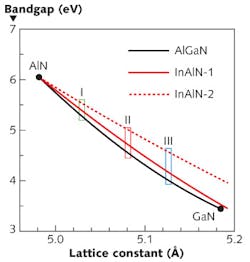
Application-oriented nitride substrates are bulk AlxGa1-xN ternary substrates with Al compositions chosen to lattice-match thick barrier layers. In some cases, an Al composition could be found where a fairly broad spectral region can be covered by a single AONS. The concept can be extended into the visible and to the IR region through use of InxGa1-xN ternary substrates.7 No ternary nitride substrates currently exist. The challenges are balanced by the potential benefits for a range of electronic and photonic devices based on nitride compounds.
REFERENCES
1. H. Hirayama et al., Appl. Phys.Exp., 3, 031002 (2010).
2. M. Kneissl et al., Semicon. Sci. Technol., 26, 014036 (2010).
3. J.R. Grandusky et al., Appl. Phys.Exp., 3, 072103 (2010).
4. T.K. Sharma et al., Phys. Rev. B, 84, 035305 (2011).
5. T.K. Sharma, E. Towe, J. Appl. Phys., 109, 086104 (2011).
6. T.K. Sharma, E. Towe, J. Appl. Phys., 107, 024516 (2010).
7. T.K. Sharma, E. Towe, App. Phys. Lett., 96, 191105 (2010).
Elias Towe is with the Department of Electrical and Computer Engineering, Carnegie Mellon University, Pittsburgh, PA; e-mail: [email protected]; www.cmu.edu. Formerly with CMU, Tarun K. Sharma is now with the Semiconductor Laser Section, Raja Ramanna Centre for Advanced Technology, India.