TERAHERTZ IMAGING: Terahertz reflectometry images faults in silicon chips
MICHAEL NAGEL and HEINRICH KURZ
The steadily growing complexity of integrated-circuit (IC) technology—for example, emerging 3D through-silicon-via (3D-TSV) technology—is pushing the available inspection and fault-analysis tools to their limits.1 Among the nondestructive methods, time-domain reflectometry (TDR) is considered to be an exceptionally fast method for fault detection in electronic packages. Today’s TDR systems—also called “closed-loop radar”—are generally all-electronic and use a step or pulse generator and a high-bandwidth oscilloscope as the main components.2 The electromagnetic signal is transmitted through a high-frequency cable and a probe tip to the device under test (DUT). Every discontinuity at the transmission path within the DUT causes a part of the injected signal to be reflected. By monitoring these reflections in the time domain, it is possible to detect structural defects and distinguish functional from defective structures.
The spatial resolution dmin of a TDR system is directly linked to the rise time τrise of the injected signal by dmin = τrise ×c / 4 √ εr,eff, with c being the speed of light and εr,eff the relative effective permittivity of the transmission line. With a measured τrise = 11.1 ps high end, all-electronic systems can only reach a resolution of approximately dmin = 365 µm (εr,eff = 5).3 To surpass this limit and enable inspection of small-scale chip-level structures or advanced packages, it is necessary to switch from all-electronic to ultrafast optoelectronic technology.
A first femtosecond-laser-driven optoelectronic TDR system for fault isolation was recently introduced by Intel (Santa Clara, CA).4 With this system, a substantial improvement over all-electronic systems was achieved with τrise = 5.7 ps. However, a main bottleneck within this system—which prevents reaping the full benefits of optoelectronic sub-picosecond-range switching speeds—is brought about by the waveguide and probe components that are required for signal transmission between the optoelectronic pulse-generation/detection devices and the DUT. Frequencies above 110 GHz are not transmitted by these components, and hence the majority of resolution power is lost within the TDR system.
As we recently demonstrated, this bottleneck can now be effectively eliminated by novel micromachined probe tips applied for broadband photoconductive (PC) pulse generation and detection immediately at the DUT.5 An unprecedented TDR signal rise time of τrise = 1.1 ps has been achieved by this advanced optoelectronic system. In contrast to earlier configurations, the probes can also be used in a contact-free mode through capacitive probe/waveguide coupling. This mode is considered to be an important extension of standard TDR systems, as it can be applied to accelerated fault localization through spatiotemporally resolved field mappings of suspicious chip regions, as opposed to a single time-domain-based analysis.
Measurement system
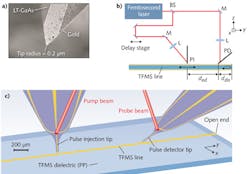
To demonstrate the capability of the system for TDR-based fault isolation, a thin-film microstrip (TFMS) line with known transmission characteristics in the terahertz range is used as the DUT.6 The optoelectronic demonstration system is based on a classic pump/probe setup for time-domain measurement (see Fig. 1). The main components are a Ti:sapphire femtosecond laser with a center wavelength of 780 nm, 150 fs full-width at half maximum (FWHM) pulsewidth, and 78 MHz repetition rate, and two micromachined identical PC probe tips. Using a beamsplitter (BS), the output beam of the laser is split into a pump and a probe beam, both having an average power of 4 mW. The pump beam is focused on a pair of biased PC switches that are integrated into the first probe. This probe is used for pulse injection (PI) into the DUT. The biased PC switches are formed by two 5-µm-wide gaps between two titanium/gold-based strip lines and a continuous center strip line running to the tip apex. These planar electrode structures are integrated on a 1.3-µm-thick cantilever of PC gallium arsenide material grown by molecular-beam epitaxy at low temperatures featuring ultrashort lifetimes (τc = 250 fs) of optically generated charge carriers.7
In the spatial configuration of the probe tips and the DUT used during the measurement, both probe tips are kept at a 10 µm distance above the TFMS line. The lateral probe-to-probe tip distance of 1 mm is kept fixed throughout all measurements. Pulses generated at the pair of PC switches (symmetrically biased against the center line) are guided along the center line of the probe. The signal is capacitively coupled from the probe tip to the TFMS line. From the coupling position, the pulse propagates in two antiparallel directions along the TFMS line. The second probe tip—the pulse-detection (PD) tip—is placed above the TFMS line section at a shorter distance to an open end. With this probe, the injected and reflected signals are sampled in the time domain. A linear mechanical stage controlling the optical length of the probe beam is used to sweep the time delay of the optical-probe pulses, which are focused at the PC of this probe. To increase the signal-to-noise ratio, a rectangularly modulated bias voltage (3 V peak-to-peak at a frequency of 700 Hz) and lock-in amplifier detection are used.
Experimental results
All-electronic TDR measurements are usually restricted to the time domain. The localization of a fault based only on this data can be a highly demanding task in complex DUT structures (with the occurrence of simultaneous reflections from distributed discontinuities). The raster-imaging capability of the discussed probes is, however, an important additional function that is very helpful in localizing faults. This operation is demonstrated through spatially resolved measurements of the electric field of the pulse reflected at the open-end region of the TFMS line, resulting in field mappings at three different time delays (see Fig. 2). The configuration of the probes and the whole setup was kept fixed during the measurement except for the DUT, which was scanned laterally in two dimensions.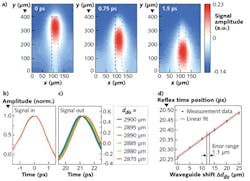
The left diagram in Fig. 2a shows the first fully evolved reflection at the open end at 0 ps (the lateral boundaries of the TFMS line are marked by a dashed line). The location where the reflection is generated as well as the propagation dynamics and the confinement of the signal are clearly visible from the data. Considering the time-domain data of the injected and reflected signal at the TFMS line as seen in Fig. 2b and 2c, respectively, an ultrashort rise time of 1.1 ps (determined at the 10%–90% levels of the rising signal edge) is obtained—an order of magnitude shorter than available from state-of-the-art all-electronic systems. It is expected that the rise time can be further reduced to close to carrier lifetimes through careful probe-design optimization, taking into account DUT-specific coupling conditions.
The location accuracy is quantified by taking TDR scans at varying probe-to-end distances (ddo) in a range of 2875–2900 µm in 5 µm steps. The time position and slope of the incoming signal are virtually constant, as expected, as seen in Fig 2b. A residual time base error of approximately ±5 fs is measured for the incoming signal. For the reflected signals (signal out) seen in Fig. 2c, very uniform signal slopes shifted toward earlier times for decreasing ddo are observed. Plotting the signal edge position versus the change in ddo, as seen in Fig. 2d, shows a standard deviation from an idealized linear devolution of 2.6 fs and a maximum deviation of ±5.1 fs. This translates into a spatial location accuracy of ±0.55 µm.
In a proof-of-principle investigation, we have demonstrated that micromachined probes equipped with ultrafast photoconductive switches can be effectively applied to unleash the extraordinary resolution power of optoelectronic systems for TDR-based fault-analysis applications. Other applications in the field of terahertz near-field microscopy—for example, in semiconductor material inspection or biomolecular sensing—are also foreseen.
REFERENCES
1. J.H. Lau, “Evolution, Challenge, and Outlook of TSV (Through-Silicon Via) and 3D IC/Si Integration,” IEEE Intl. Conf. on Electron. Packaging—ICEP, Nara, Japan (April 13–15, 2011).
2. Application Note 1304-1, Agilent Technologies; www.agilent.com.
3. K. Schoen, Picosecond Pulse Labs, www.picosecond.com (2004).
4. Y. Cai et al., Proc. 60th ECTC 2010, Las Vegas, NV, USA, 1309–1315 (2010).
5. M. Nagel et al., Opt. Expr., 19, 12509–12514 (2011).
6. M. Nagel et al., Microwave Opt. Technol. Lett., 29, 97 (2001).
7. M. Wächter et al., Appl. Phys. Lett., 95, 041112 (2009).
Michael Nagel is researcher and product developer and Heinrich Kurz is managing director at AMO GmbH (Aachen, Germany); e-mail: [email protected]; www.amo.de.