Shuji Nakamura's seemingly single-handed invention of practical gallium nitride–based blue and UV lasers and light-emitting diodes (LEDs) during his stint at Nichia (Kaminaka, Japan) has made him one of the few optoelectronics researchers to receive publicity in the general press (Nakamura is now at the University of California, Santa Barbara). Most recently, he made the news when he was awarded $189 million in a court battle with Nichia over the rights to his invention (see Laser Focus World, March 2004, p. 53). In contrast, the story of the attempts to make workable light sources based on the UV-emitting semiconductor zinc oxide (ZnO) has not caught the attention of the general media.
Achievements in the field of ZnO emitters include the production of laser light in random microcrystalline structures of optically pumped ZnO (see Laser Focus World, August 1998, p. 22), in collections of optically pumped ZnO nanowires (see Laser Focus World, August 2001, p. 17), in optically pumped single nanowires (see Laser Focus World, January 2002, p. 15), and in low-efficiency electrically pumped transparent LEDs (see Laser Focus World, December 2000, p. 59). The advances toward practicality in this field are incremental, perhaps as a result of the difficulty in getting the material to emit light when electrically pumped (the transparent LED is actually a hybrid, using ZnO as the n-type material but strontium cuprate as the p-type material).
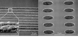
But researchers are successfully chipping away at other hurdles to the fabrication of practical ZnO emitters and devices. For example, a group at the Osaka Municipal Technical Research Institute (OMTRI; Osaka, Japan) and Utsunomiya University (Tochigi, Japan) is creating ZnO microstructures on silicon (Si) wafers by just-above-room-temperature electrodeposition (see figure).1 The structures emit light in the UV and visible—although only when optically pumped.
The Si-wafer substrate is first coated with a 20-nm-thick film of titanium and a 500-nm-thick (111)-oriented layer of gold (direct deposition of ZnO on Si is not practical because of the large lattice mismatch between the two materials). A final photoresist layer is exposed through a photomask to create the desired microstructure pattern. A 200-nm-thick layer of (0001)-oriented ZnO is electrodeposited from a zinc nitrate hydrate aqueous solution at a temperature of 333°C onto the exposed gold areas. Finally, the remaining photoresist is removed.
Lines 5 µm wide and microdot arrays with 5-µm-diameter dots have been fabricated. The features are made up of 600-nm-wide hexagonal columnar grains aggregated together; the columns grow normal to the wafer surface and have smooth tops.
A photoluminescence spectrum shows peaks at 391, 454, and 536 nm and a lower-level continuum in between. The photoluminescence is a durable property of the ZnO structures. Although the emission spectrum changed slightly in shape over six months of exposure to ambient air at room temperature, the amount of light emitted remained high.
The technique shows promise for integrating ZnO optoelectronics with standard Si integrated-circuit technology. Because ZnO can also serve as a solar-blind photodetector, obtaining electrically pumped light from ZnO/Si devices may not be necessary for their practical use.
REFERENCE
- Masanobu Izaki et al., Appl. Phys. Lett. 83, 4930 (Dec.15, 2003).

