A fast modulator made of silicon (Si) may make researchers take another look at the material, which has been largely forsaken by the optoelectronics industry in favor of other semiconductors with more favorable light-manipulating properties. Optoelectronics research has been focused on III-V compound semiconductors because Si is optically handicapped: the material's indirect bandgap doesn't provide a conventional method for light emission, and Si optoelectronic modulators have been far slower in the past than materials such as lithium niobate.
Ansheng Liu and others at Intel (Santa Clara, CA, and Jerusalem, Israel) have now reported producing an optical modulator in Si that operates much faster than the previous record, and even faster than was theoretically possible for a Si waveguide modulator.1 The group demonstrated an all-Si optical modulator with a bandwidth of more than 1 GHz. The technology can be created alongside (and integrated with) conventional CMOS microelectronics on a single Si substrate.
Silicon is an attractive material because the electronics industry has driven research, growth, and fabrication technologies for decades—compared to other semiconductors, Si is a well-understood, inexpensive material with a huge installed base of processing equipment. The poor light-manipulating properties of Si, however, have led the optoelectronics industry to develop gallium arsenide, indium phosphide, and other compound semiconductors.
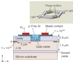
The researchers made an intensity modulator from a Mach-Zehnder interferometer, in which each arm incorporated a phase modulator. The phase modulator is made of an n-doped silicon-on-insulator (SOI) slab and a p-doped polysilicon rib with a thin gate oxide sandwiched between them (see Fig. 1). The devices were fabricated in an existing CMOS production facility at Intel. The device is a single-mode polarization-sensitive device at 1.55 µm.
Plasma-dispersion effect
The phase modulator operates much more quickly than previously reported Si modulators because it uses a different mechanism. Instead of changing the refractive index using thermal effects or depending on the movement of free carriers, the device changes the refractive index by the free-carrier plasma-dispersion effect.2
When a positive charge is applied to the polysilicon, charge carriers accumulate at the gate, which modifies the refractive index, which in turn creates an optical phase shift in light passing through the waveguide. The advantage of using a metal-oxide-semiconductor-capacitor phase shifter, say the researchers, is the high achievable modulation speed, as there are no slow carrier generation and/or recombination processes involved in the accumulation operation.
They found that the speed of the device depends on the resistance of the silicon and polysilicon, and therefore they chose doping concentrations to alter the resistance and produce a high-speed device. They found (as predicted) that the phase shift is linearly dependent on both the drive voltage and the length of the device. The modulator's on-chip loss is about 6.7 dB, mostly from absorption in the polysilicon waveguide.
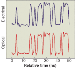
When a 1-Gbit/s 3.5-V digital pulse pattern (atop a 3-V direct-current bias) was applied to the single-arm 2.5-mm-long phase shifter, the optical output reproduced the bit pattern (see Fig. 2).Next step
Further research to improve device characteristics will concentrate on increasing transmission and reducing the size of the waveguides.
The researchers believe they may be able to reduce the loss by as much as 5 dB by replacing the polysilicon with single-crystal silicon. They are actively working on using the epitaxial lateral overgrowth technique to this end. The group is also investigating use of a graded doping profile and the potential for reducing losses and drive voltage by reducing the thickness of the gate oxide.
REFERENCES
- A. Liu et al., Nature 427 (Feb. 12, 2004).
- R. A. Soref and B. R. Bennett, IEEE J. Quant. Electron. QE-23, (1987).

