Terahertz radiation carries information
Researchers at the Technical University of Braunschweig (Braunschweig, Germany) and the University of Manchester Institute of Science and Technology (Manchester, England) have demonstrated transmission of information by modulating terahertz waves. With a frequency between that of mid-IR light and microwaves, terahertz radiation is interesting in that it can be formed and manipulated using either optical or radio methods; the methods can be combined, such as using a refractive or diffractive lens to focus terahertz radiation from a terahertz radio source.
The modulator structure is based on a well-established concept used in high-frequency transistors in which a thin layer of electrons is removed by applying an external voltage. The removal of the electron layer increases the transmission of terahertz radiation through the modulator structure, allowing the terahertz radiation to be adjusted via the applied voltage. In the first test of this concept, a modulator was placed in a terahertz emitter-receiver system and was driven by the analog output from a CD player. The signal from the detector antenna was transmitted at a telephone-like quality. The group is trying to optimize the modulator structures to achieve higher modulation depths and higher operational frequencies. Contact Martin Koch at [email protected].
QD and QW lasers face off
Semiconductor quantum-well (QW) lasers are the workhorses of the laser-diode world. Semiconductor quantum-dot (QD) lasers, on the other hand, remain largely in research, as their predicted beneficial qualities—a narrow gain spectrum, no carrier-induced change in refractive index, and a zero linewidth-enhancement factor (a) at the gain peak—are hard to achieve so far. Now, a group at the University of New Mexico (Albuquerque, NM) is comparing QW and QD lasers of identical design (except for the presence or absence of QDs) to each other.
The lasers are based on gallium arsenide (GaAs) with aluminum and indium (In) in some layers; the QDs are of InAs. The researchers found that a was almost independent of energy over s 20-meV range in the QD laser, and up to two times smaller in the QD laser than in the QW laser for low-energy transition. The material differential gain and material differential carrier-induced refractive index were three times smaller in the QD laser; a sixfold decrease of the modal differential carrier-induced refractive index in the QD lasers shows their potential for applications needing reduced frequency chirp. Contact Alexander Ukhanov at [email protected].
Attosecond pulses probe atoms' inner dynamics
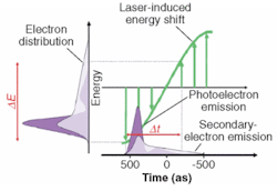
Probing transient events in the interior of an atom with light requires pulse durations that are on the order of the 150-attosecond (as) orbit time of an electron. Scientists at the Vienna University of Technology (Vienna, Austria), the Max Planck Institute for Quantum Optics (Garching, Germany), and the University of Bielefeld (Bielefeld, Germany) are generating 250-as x-ray pulses and using them to excite electron shells of the irradiated atoms. The durations and time variations of the resulting electron emissions provide information on the evolution of excitation and relaxation processes inside the atom.
The x-ray pulses are generated from neon atoms by 5-fs, 750-nm laser pulses with controlled waveforms that produce high-order harmonics. The pulses are focused into the atoms being analyzed—another neon-gas jet. The transient electron events are measured using a form of streak-camera imaging, in which the rising electric field of the laser light sweeps the beam of ejected electrons in energy rather than space, revealing the x-ray photoelectrons as well as secondary electrons. The technique allows direct measurement of the evolution of processes inside the electron shell of atoms with a resolution of approximately 100 as. Contact Ferenc Krausz at [email protected].
Photon-detector refrigerator cools to 100 mK
Some photodetectors must be cooled to reduce electrical noise; a small subset of these requires chilling to close to absolute zero. For example, certain x-ray photon sensors—useful in spectroscopy for the semiconductor industry—require cooling to about 100 mK. While pumped-helium refrigerators can reach 300 mK, that last 200-mK drop in temperature is conventionally achieved with expensive and complex adiabatic-demagnetization refrigerators. Now, researchers at the National Institute of Standards and Technology (Boulder, CO) have developed a thin-film solid-state refrigerator that goes the last few millikelvins in a simple manner.
The device contains biased normal-metal/insulator/superconductor (NIS) junctions. While previous NIS-based refrigerators had trouble attaining adequate cooling power, the new device scales naturally to larger sizes and powers and more-complex geometries. The researchers achieved this by using a normal electrode of manganese-doped aluminum to suppress superconductivity, reversing the traditional NIS layout; the superconducting electrode then becomes very thick, decreasing quasiparticle density near the junctions.
The fabricated device cools from 260 to131 mK; an improved device should cool from 300 to 98 mK. The researchers are fabricating an integrated x-ray sensor and refrigerator with the improved device. Contact Anna Clark at [email protected].
Quantum-dot transistor counts photons
A quantum-dot field-effect transistor (QDFET) is at the heart of a low-noise single-photon detector developed at Toshiba Research Limited and Cavendish Laboratory (both of Cambridge, England) that has a microsecond response time. The active region of the cryogenic (4.2 K) device contains a few hundred indium arsenide quantum dots—a number low enough that, when a photogenerated hole in the conducting channel recombines with an electron trapped in a dot, a measurable increase in current occurs.
A cryogenic amplifier is placed very close to the QDFET, lowering the lead capacitance enough that the detector can be operated at megahertz rates. The transistor has a dot density of 1.4 × 10¹⁴ m-2 and is biased with 20 mV across the source drain and with a variable voltage between the gate and drain. In a test, the device was illuminated with pulses from a 684-nm-emitting laser diode, with each pulse averaging 0.35 photons per 1 µm2, which is the area of the detector. The laser operated at 400 kHz for 20,000 pulses. The maximum detection efficiency of 0.14% (internal quantum efficiency of 10%) occurred at a discriminator level of 50 mV; the dark count rate was less than 10-8 ns-1 at a 70-mV level and 0.045% efficiency. Contact Beata Kardynal at [email protected].
Brownian MOONs measure viscosity
The rotational viscosity of fluids influences industrial as well as life processes. Measuring rotational viscosity on the microscopic scale is important, because many fluids have a viscosity that depends on the scale of the measurement probe; in other words, the size of the probe is relevant to the scale of the processes of interest. Researchers at the University of Michigan (Ann Arbor, MI) have developed an optical nanoprobe that measures viscosity at the micron size scale and time scales on the order of a few seconds.
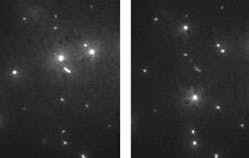
Called Brownian modulated optical nanoparticles (Brownian MOONs), the probes are simply fluorescent nanospheres half-coated with a metal film to block that side's fluorescence. In operation, Brownian motion causes the spheres to rotate erratically; under a microscope, the picture is of many fluorescent dots that wink on and off (for example, the bright dot at left disappears 2 s later at right). The Brownian MOONs have been made in sizes ranging from 200 nm to 4 mm in diameter; an aluminum or gold coating 20 nm thick renders one side opaque. The MOONs may be used in immunoassay procedures and intracellular chemical sensors. Contact Raoul Kopelman at [email protected].
Random-wavelength ceramic laser emits in stable transverse mode
In an example of a technological development that as yet has no practical application (but may someday), researchers at Nanyang Technological University (Singapore) and the University of Electro-Communication (Tokyo, Japan) have developed a diode-pumped solid-state laser that, within a 2-nm bandwidth, displays a random wavelength spectrum while maintaining fixed and well-defined transverse modes. The phenomenon occurs as a result of strong reabsorption of the laser light in the gain medium.
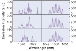
The gain medium is a ytterbium (Yb)-doped yttrium oxide ceramic emitting at approximately 1078 nm; laser-diode pump light at 640 nm was focused to a beam diameter of 200 mm within the water-cooled 3-mm-thick ceramic slab. For comparison, a conventional single-crystal Yb:YAG laser was fabricated of similar dimensions. The spectrum of the ceramic laser varied wildly and randomly in time (left, top to bottom), while the single-crystal laser showed a conventional spectrum of a few stable longitudinal modes (right, top to bottom). In addition to maintaining a well-defined and unchanging beam profile, the random ceramic laser maintained a constant continuous-wave output power. Increasing the pump power shifted the bandwidth center by 8 nm. Contact Dingyuan Tang at [email protected].
Corner-detection algorithm prunes false candidates
Corners are important parts of the geometry of objects within an image; consequently, corner-detection algorithms are important to image processing, in which the confusing information in a real image is reduced to something a computer can analyze. Although corners are easy for people to pick out, corner-detection algorithms tend to find far too many features that they decide are corners. In the interest of reducing the excess, while not missing true corners, researchers at the University of Kent (Canterbury, England) have developed a new algorithm that prunes candidate corners early, reducing computational load.
In the cascaded candidate-pruning (CCP) algorithm, corner candidates are first found as the intersection of edges. A non-maxima suppression is then applied to eliminate false corners resulting from multiple responses of the gradient operator. Next, the high gradients caused by diagonal edge pixels are suppressed through an eigenvalue computation. Finally, corners that are too close to each other are suppressed. In a test against other algorithms in which corners are tracked across different images, the CCP algorithm showed high stability, outperforming the other algorithms while saving computational time. Contact Farzin Deravi at [email protected].
Single polymer serves both as transistor and emitter in active pixel
Active-matrix flat-panel displays that use organic light-emitting diodes (OLEDs) as their elements have a transistor at each OLED pixel for signal processing. Because semiconductors that work well for transistors are not usually the same as those that work well for OLEDs, integrating transistors and OLEDs requires many steps. If the two types of components could share the same semiconductor, fabrication would be much simpler. Researchers at National Chiao Tung University and National Tsing Hua University (both of Hsinchu, Taiwan) and National Taipei University of Technology (Taipei, Taiwan) have demonstrated just this sort of device.
The amorphous organic semiconductor poly[2-methoxy-5-(2'-ethyl-hexyloxy)-1,4-phenylene vinylene], or MEH-PPV is a conjugated polymer already used for some OLED devices; it emits at about 570 nm. The researchers used this same material to also fabricate a metal-oxide field-effect transistor (MOSFET), creating a single active pixel on a glass substrate. The horizontal mobility for the MOSFET in the thin film is three orders of magnitude larger than the vertical mobility for the OLED. The 100 × 200-µm OLED has a brightness of 100 cd/m2 at a current of 400 nA. Contact Hsin Fei Meng at [email protected].


