Using EUV lithography, IBM research alliance produces first 7-nm-node test chips

July 9, 2015
Silicon-germanium channel transistors are formed via lithography at a 13 nm wavelength.
(Darryl Bautista/Feature Photo Service for IBM)
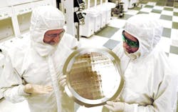
Michael Liehr (left) of SUNY Polytechnic Institute's Colleges of Nanoscale Science and Engineering and Bala Haran (right) of IBM Research inspect a wafer containing 7-nm-node test chips in a clean room in Albany, NY. IBM Research, working with alliance partners at SUNY Poly CNSE, has produced the semiconductor industry's first 7-nm-node test chips with functional transistors.

An alliance led by IBM Research (Albany, NY; NYSE:IBM) has produced the semiconductor industry's first 7-nm-node test chips with functioning transistors. While computer chips at the 14 nm node (already appearing in leading-edge commercial products) and at the 10 nm node (in development by Intel) rely on silicon (Si) as the semiconductor, chips at the 7 nm node will likely not be based solely on silicon. III-V semiconductors such as those based on gallium arsenide are one possibility; however, the new IBM chip relies partly on Si, combining the material with germanium (Ge) to form SiGe channel transistors.

EUV gets real use

Extreme-ultraviolet (EUV) lithography was required for a number of levels (layers) on the chip. Rather than the 193 nm excimer-laser light used for leading-edge conventional lithography, EUV lithography is based on the 13 nm light produced when droplets of tin are irradiated with light from a carbon dioxide (CO2) laser. ASML (Veldhoven, Netherlands) is developing an EUV lithograpic scanner for exposing 7-nm-resolution patterns on chips; light sources are being developed by Cymer (San Diego, CA) and Gigaphoton (Oyama, Japan), while optics are being designed and fabricated at Zygo Extreme Precision Optics (Richmond, CA), among other places. ASML acquired Cymer in 2012.

IBM's achievement, accomplished in partnership with GLOBALFOUNDRIES and Samsung at SUNY Polytechnic Institute's Colleges of Nanoscale Science and Engineering (SUNY Poly CNSE), could result in the ability to place more than 20 billion transistors on a chip. The result is part of IBM's $3 billion, five-year investment in chip R&D, which it announced in 2014.

IBM and SUNY Poly have built a partnership at the multibillion dollar Albany NanoTech Complex, highlighted by the institution's Center for Semiconductor Research (CSR), a $500 million program that also includes leading nanoelectronics companies. The CSR is a long-term, multiphase, joint R&D cooperative program on future computer-chip technology thatprovides student scholarships and fellowships at the university.

For more info on the SUNY Polytechnic Institute, see www.sunycnse.com and www.sunypoly.edu

For more info on IBM Research, see www.research.ibm.com

Source: http://www-03.ibm.com/press/us/en/pressrelease/47301.wss
About the Author

John Wallace | Senior Technical Editor (1998-2022)

John Wallace was with Laser Focus World for nearly 25 years, retiring in late June 2022. He obtained a bachelor's degree in mechanical engineering and physics at Rutgers University and a master's in optical engineering at the University of Rochester. Before becoming an editor, John worked as an engineer at RCA, Exxon, Eastman Kodak, and GCA Corporation.

Sponsored Recommendations

Request a quote: Micro 3D Printed Part or microArch micro-precision 3D printers

April 11, 2024
See the results for yourself! We'll print a benchmark part so that you can assess our quality. Just send us your file and we'll get to work.

Request a free Micro 3D Printed sample part

April 11, 2024
The best way to understand the part quality we can achieve is by seeing it first-hand. Request a free 3D printed high-precision sample part.

How to Tune Servo Systems: The Basics

April 10, 2024
Learn how to tune a servo system using frequency-based tools to meet system specifications by watching our webinar!

Precision Motion Control for Sample Manipulation in Ultra-High Resolution Tomography

April 10, 2024
Learn the critical items that designers and engineers must consider when attempting to achieve reliable ultra-high resolution tomography results here!

Voice your opinion!

To join the conversation, and become an exclusive member of Laser Focus World, create an account today!