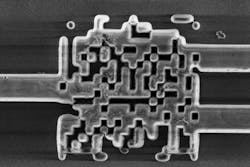
Engineers at the University of Utah (Salt Lake City, UT) have developed an ultracompact beamsplitter—the smallest on record—for dividing light waves into two separate channels of information. The device brings researchers closer to producing silicon photonic chips that compute and shuttle data with light instead of electrons. Electrical and computer engineering associate professor Rajesh Menon and colleagues describe their invention in Nature Photonics.
RELATED ARTICLE: Silicon photonics evolve to meet real-world requirements
Silicon photonics could significantly increase the power and speed of machines such as supercomputers, datacenter servers, and the specialized computers that direct autonomous cars and drones with collision detection. Eventually, the technology could reach home computers and mobile devices and improve applications from gaming to video streaming.
Photons of light carry information over the Internet through fiber-optic networks . But once a data stream reaches a home or office destination, the photons of light must be converted to electrons before a router or computer can handle the information. That bottleneck could be eliminated if the data stream remained as light within computer processors.
The small polarization beamsplitter (which looks somewhat like a barcode) is fabricated on top of a silicon chip that can split guided incoming light into its two components. Before, such a beamsplitter was over 100 by 100 microns. Thanks to a new algorithm for designing the splitter, Menon’s team has shrunk it to 2.4 by 2.4 microns, or one-fiftieth the width of a human hair and close to the limit of what is physically possible.
The beamsplitter would be just one of a multitude of passive devices placed on a silicon chip to direct light waves in different ways. By shrinking them down in size, researchers will be able to cram millions of these devices on a single chip.
Potential advantages go beyond processing speed. The Utah team’s design would be cheap to produce because it uses existing fabrication techniques for creating silicon chips. And because photonic chips shuttle photons instead of electrons, mobile devices such as smartphones or tablets built with this technology would consume less power, have longer battery life and generate less heat than existing mobile devices.
The first supercomputers using silicon photonics—already under development at companies such as Intel and IBM—will use hybrid processors that remain partly electronic. Menon believes his beamsplitter could be used in those computers in about three years. Data centers that require faster connections between computers also could implement the technology soon, he says.
SOURCE: University of Utah; http://unews.utah.edu/news_releases/silicon-photonics/?

